Whatever Happened to “Programmable” Analog?
I recently received an email via LinkedIn from someone asking about an article I wrote back in 2001 asking if there were any updates. Wow – talk about the past coming back at you! The article was on programmable analog and looked at a different design option for analog signal chain functionality.
Since one of my many peeves with general news coverage these days is their lack of story follow-up coverage (you get live, dramatic report of the arrest, but rarely the results of the trial), and since it has been nearly two decades since that article appeared, it seemed worthwhile to re-visit the topic.
First, though, we need a clarifying definition. There are many programmable analog ICs out there where the user can set some operational parameters or functions such as bandwidth or sampling rate using pin-strapping, discrete resistors, or software driven via an I2C/SPI port. However, these are not what I mean by “programmable” in this context.
Instead, I’m referring to the analog complement to the field-programmable gate array (FPGA), a component which has a large array of uncommitted digital gates and functions. These can be interconnected as needed to create the final circuit topology and thus deliver extremely complicated digital systems; FPGAs with over a million gates are now common. There’s no question that FPGAs have become a major force, for reasons I don’t need to explain to this audience; and the new product introductions just keep on coming.
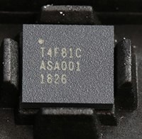
 Figure 1: The T4F81C FPGA from Efinix is built on SMIC’s 40 nanometer (nm) process and has less than 150 microamps (µA) typical core leakage at 1.1 volts. (Image source: Efinix)
Recently introduced is the T4F81C2 Trion™ from Efinix. The FPGA is built on SMIC's 40 nm process and comes in an 81-ball BGA package (Figure 1).
The T4F81C features the high-density, low-power Efinix Quantum™ fabric wrapped with an I/O interface in a small footprint package. It’s targeted at mobile, consumer, and IoT edge markets that need low power, low cost, and a small form factor. The T4F81C’s highlights include:
- Built on SMIC's 40 nm process
- Has less than 150 µA typical core leakage current at 1.1 volt
- Features high-performance I/O supporting 1.8 volt, 2.5 volt, and 3.3 volt single-ended I/O standards and interfaces
- Provides flexible on-chip clocking
- Has device configuration options including standard SPI and JTAG interfaces
The FPGA introductions will continue as the technology continues to evolve and address more diverse requirements and applications, but not very many programmable analog devices have emerged of late.
Seems like a good idea, so…?
It may seem that there’s a need for an analogous IC with numerous uncommitted analog functions. In theory, it could provide the entire analog signal chain for sensor interface, signal conditioning, filtering, and even I/O to a host processor (as just one example). This field-programmable analog array (FPAA) could even be configured at the OEM production line to provide functions needed for different products within a family or series, so the BOM would be common across multiple products, Also, if changes in the analog chain functionality were needed, they could be implemented without the dreaded pc board re-spin, with its associated delays and uncertainties.
The reality is that programmable analog of this type hasn’t caught on much with the engineering design community. Looking at the vendors I cited in that 2001 article, some are gone, and some have been absorbed by other IC firms – that’s fairly normal in this industry and not itself noteworthy – but none have developed any sort of commanding market presence. To the extent it is still even available, this class of product has a very low profile; I don’t hear of designers looking to programmable analog as a solution option for their signal chain needs.
Why hasn’t programmable analog caught on? I think it’s due to the inherent, unavoidable nature of analog circuitry and the functions it provides. If you look at the most basic analog building block functions such as op amps and comparators, most vendors offer dozens or even hundreds of these in their portfolio, (see, “My Head is Spinning: Why So Many Op Amps?”). The reason is that each model is tuned by design, fab process, and test/trim to provide a unique combination of performance attributes. One op amp, for example, may have outstanding low-noise performance but more offset drift than another somewhat similar one that has higher noise.
It’s about the multidimensional tradeoffs
The designer must assess the tradeoffs and decide what performance price to pay in order to get the desired performance with the ranked priorities. Other op amps will offer different combinations across key static and dynamic specifications, with some being outstanding in one or two areas but only so-so in others; other devices may be “pretty good” across most specifications but not really, truly great in any individual one. So, which is the “right” one for the design?
As always, the answer is “it depends” based on ranking of design priorities and weighting of tradeoffs. Think of the many parameters which are used to assess basic op amps such as speed, voltage offsets, bias current, temperature drift, bandwidth, noise, dissipation, gain, drive capability, voltage range, and, well, you get the idea: it’s a very long list.
Further, if you step back and look at the bigger picture, unlike the digital world of the FPGA, most analog signal chains just don’t have many functional blocks, and the ones they have usually differ dramatically from each other. The critical characteristics of the analog block change with the signal’s location: what you need in a sensor-facing interface is not what you need further along at the bandpass filter, for driving a load, or for the processor I/O.
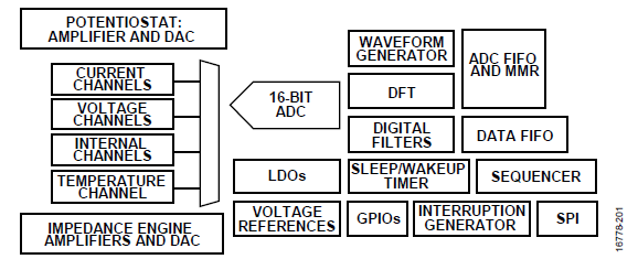
For example, consider Analog Devices’ AD5940, a niche IC which provides a high-precision impedance and electrochemical front-end for chemical lab setups (Figure 2). The AD5940 comprises a large number of analog and digital functions, but the analog ones are the most varied, with specifications that are carefully established to be compatible with the electrochemical sensors they support.
 Figure 2: The simplified block diagram of the AD5940. (Image source: Analog Devices)
While it does have an internal analog-to-digital converter (ADC) and even a microcontroller for internal management, the most sensitive part of the design is the section which interfaces with the specialized lab electrodes of potentiostats, including op amps with near-zero bias current and programmable-gain amplifiers (PGAs). The analog functions within a more general FPAA would not have the sensitive characteristics needed.
Conclusion
Despite its initial attractiveness in principle, the reality is that a general array of analog blocks can’t meet the diverse needs of many applications. The compromises would be unacceptable, while the actual benefits in BOM complexity, pc board real estate, and other design factors would not be enough to make it worthwhile.
For most analog designs, a few (and usually different) ICs carefully chosen to be best-fit for each part of the signal chain is the better design approach. The good news? There’s no shortage of good choices for every stage of that chain.

Have questions or comments? Continue the conversation on TechForum, DigiKey's online community and technical resource.
Visit TechForum


