How GaN HEMTs Can Help You Increase Power Supply Efficiency
I have a confession to make. Throughout my many years in the electronics industry, both as a hands-on circuit designer and as an editor, I have found that most engineers (including me) are not that interested in the deep-dive details of semiconductor materials, processes, and fabrication technology. Certainly, there are those who live for the annual IEEE ISSCC (International Solid State Circuits Conference) and care about process detail and innovation, and their work is important, impressive, and admirable.
However, what most design engineers really want to know is not how a device is made, but what it can do: its strengths, weaknesses, tradeoffs, and other key attributes. Stating that “My process is smaller, better, lower power, faster, and perhaps cheaper than yours,” isn’t exciting by itself; instead, it’s the resultant parts and their datasheet numbers and graphs that really matter to most potential users.
Despite this view, the reality is that process technology is important and fundamental to the advances in semiconductor performance and capabilities. That’s especially true in the current power-device arena where the commercialization of new or enhanced processes is redefining what can be accomplished with switching circuits and their systems. The applications range from small smartphone chargers to EVs and their charging stations. I could call these advances “revolutionary”, but that word is overused and has lost its true meaning.
Wide-bandgap devices at core of new capabilities
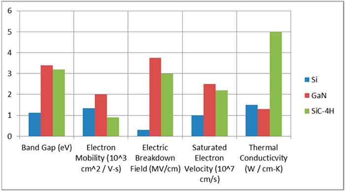
At the core of this change is the availability of wide-bandgap (WBG) power semiconductors fabricated using silicon carbide (SiC) and gallium nitride (GaN) materials and processes. The WBG devices offer multiple benefits compared to the traditional silicon (Si)-only devices and, in many cases, are supplanting them or enabling new designs that were not previously feasible (Figure 1).
 Figure 1 : The relative attributes of GaN and SiC-based power devices show that these newer WBG components have attractive figures of merit compared to silicon-only components. (Image source: Scholarly Community Encyclopedia)
Specifically, GaN-based high-electron-mobility transistors (HEMTs) are superior to conventional silicon-based devices in terms of switching frequency, power rating, thermal capability, and efficiency, all of which are crucial factors in enhancing the performance of advanced power converters. These benefits are the result of GaN’s intrinsic merits of WBG voltage, high critical-breakdown electric field, high thermal conductivity, and high electronic saturation velocity. GaN-based power switching devices can offer small “on” resistance, high current capability, and high power density.
Commercially available GaN-based power-switching devices offer an operating voltage ranging from 100 volts to nearly 1000 volts, high switching frequency, high-temperature operation, and reduced switching losses. GaN has higher figures of merit than SiC; however, the material is more difficult to crystallize and process.
HEMT is a GaN technology where elements are formed only on the surface of a substrate on which GaN crystal growth is possible. Currently, the major commercial GaN FETs are lateral HEMTs.
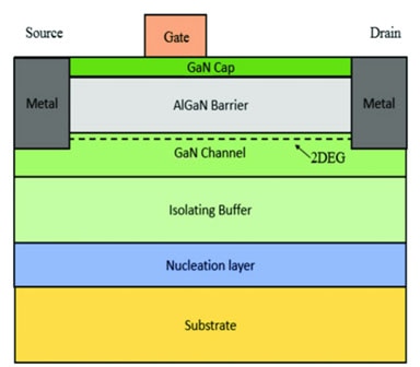
In the lateral structure of GaN FETs, there is a silicon substrate, a GaN buffer, an aluminum gallium nitride (AlGaN) barrier, three connection terminals (source, gate, and drain), a layer of passivation (protection dielectric), and a field plate extending from the source terminal (Figure 2). The heterojunction (a junction between two different semiconductors) of the AlGaN barrier and GaN buffer forms a two-dimensional electron gas (2DEG) channel.
 Figure 2 : The structure of GaN power devices shows multiple layers and a 2DEG channel through which the current flows or is cut off. (Image source: ResearchGate)
This channel has a high charge density and mobility. Current flows in the 2DEG channel, in contrast to a Si MOSFET where the channel for current flow is the depletion region between the source and drain.
Note that a standard GaN HEMT is normally “on”, which differs from a conventional MOSFET which is normally “off.” To turn a GaN HEMT to its off state, which is easier to use and preferred in most circuit designs for convenience and safety, it is necessary to deplete the 2DEG layer which, in turn, causes cessation of current flow.
As a result, GaN switching devices come in two different types: enhancement mode (e-GaN) and depletion mode (d-GaN). A depletion mode transistor is normally on and requires the use of a negative voltage applied at the gate to turn off. An enhancement mode transistor is normally off and is turned on by a positive voltage applied at the gate.
SiC versus GaN
The most significant difference between GaN and SiC lies in their electron mobility, which indicates how quickly electrons can move through the semiconductor material. Standard silicon has an electron mobility of 1500 centimeter2 per volt-second (cm2/volt-s). SiC, however, has an electron mobility of 650 cm2/volt-s, and GaN has an electron mobility of 2000 cm2/volt-s, which means that SiC's electrons are slower moving than those of both GaN and silicon.
GaN’s electrons can move over 30% faster than silicon's electrons. With such elevated electron mobility, GaN is nearly three times more suitable for high-frequency applications.
Further, GaN has a thermal conductivity of 1.3 watts/centimeter-K (watts/cm-K), which is worse than that of silicon at 1.5 watts/cm-K. However, SiC has a thermal conductivity of 5 watts/cm-K, making it nearly three times more efficient at transferring thermal loads. This feature gives SiC a strong advantage in high-power, high-temperature applications.
GaN and SiC serve different power needs in the market. SiC devices offer voltage levels as high as 1,200 volts with high current-carrying capabilities. This makes them suitable for applications such as automotive and locomotive traction inverters, high-power solar farms, and large three-phase grid converters.
In contrast, GaN HEMT devices are typically rated to 650 volts and can enable high-density converters in the range of 10 kilowatts (kW) and higher. Their applications include consumer, server, telecom, and industrial power supplies; servomotor drivers; grid converters; and EV onboard chargers and DC-DC converters.
Despite these differences, the SiC and GaN technologies have overlap in some applications below 10 kW.
Available GaN devices highlight performance
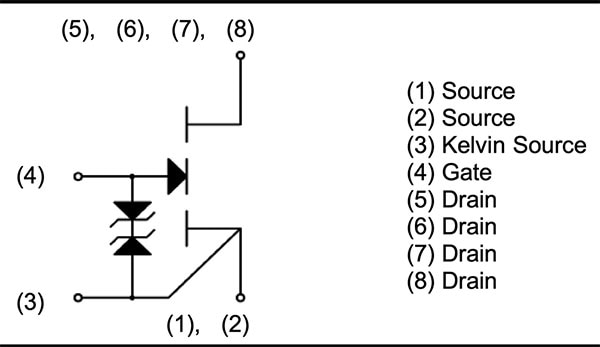
While the development of GaN-based devices took many years of lab research and development, as well as production effort, GaN devices have been in commercial production for over a decade. Two examples are the GNP1070TC-Z and GNP1150TCA-Z 650 volt GaN HEMTs from ROHM Semiconductor, both of which are optimized for a wide range of power-supply system applications (Figure 3). The GNP1070TC-Z is a 20 ampere (A), 56 watt enhancement mode device with drain-source resistance (RDS(on)) of 70 milliohms (mΩ) and a gate charge (Qg) of just 5.5 nanocoulombs (nC) (both typical). For the GNP1150TCA-Z, an 11 A, 62.5 watt device, the corresponding numbers are 150 mΩ and 2.7 nC, respectively.
 Figure 3: Shown is the inner circuit of the 20 A GNP1070TC-Z GaN HEMT, which is similar to the 11 A GNP1150TCA-Z; both are suitable for a range of 650 volt power-related applications. (Image source: ROHM Semiconductor)
These two components were jointly developed with Ancora Semiconductors, Inc., an affiliate of Delta Electronics, Inc., which develops GaN devices. They provide market-leading performance that contributes to higher efficiency and smaller size in a wider range of power supplies.
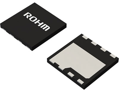
They are housed in 8-lead DFN8080K packages measuring 8 × 8 × 0.7 millimeters (mm) (Figure 4).
 Figure 4: Despite their higher current and voltage ratings, the GNP1070TC-Z and GNP1150TCA-Z GaN devices are both in packages that are just 8 mm across each side. (Image source: Rohm Semiconductor)
Conclusion
WBG power-switching devices using GaN HEMTs offer designers substantial performance advantages compared to traditional silicon-only devices. They also have distinct advantages over SiC devices with respect to operating frequency and thermal dissipation; the latter being an especially important real-world consideration. By using GaN components such as the 20 A/650 volt GNP1070TC-Z and 11 A/650 volt GNP1150TCA-Z from ROHM Semiconductor, designers can implement power converters and supplies that would otherwise not be feasible or would have severe operating limitations.
Related Content
1: Wide Bandgap Semiconductors Are Reshaping the Transportation World
2: Use SiC and GaN Power Components to Address EV Design Requirements
https://www.digikey.com/en/articles/use-sic-and-gan-power-components-ev-design-requirements

Have questions or comments? Continue the conversation on TechForum, DigiKey's online community and technical resource.
Visit TechForum


