Simplify Power Supply Design Using an Easy-to-Use Switch Mode Power Supply (SMPS) Matrix
Contributed By DigiKey's North American Editors
2024-12-19
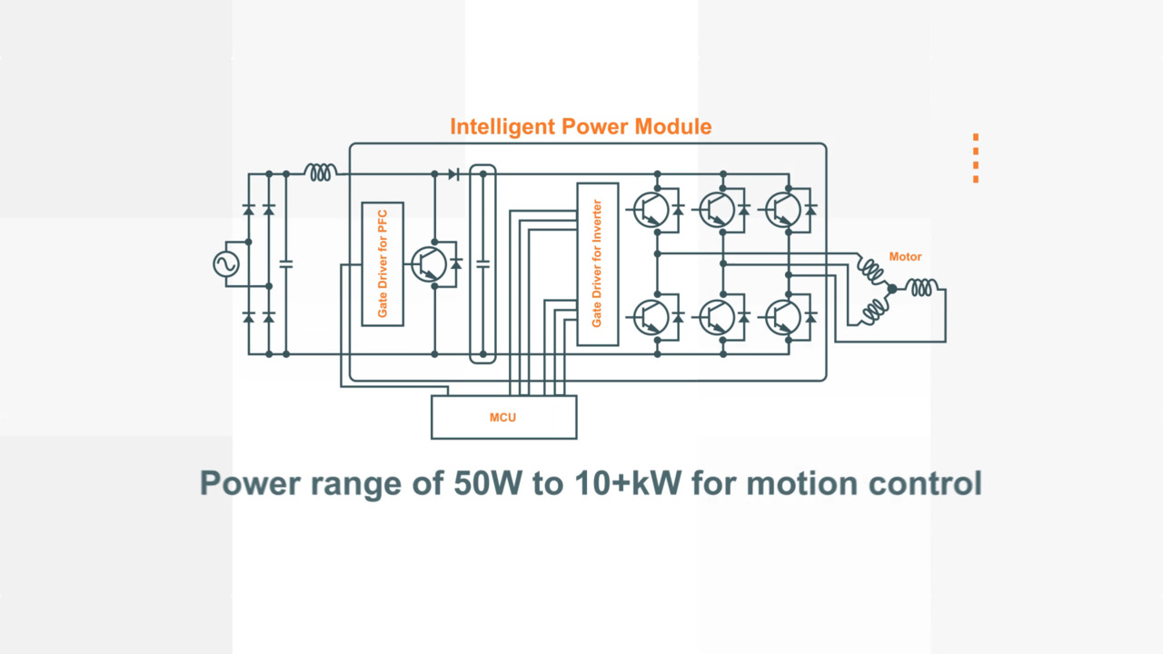
Designers of electronic products or devices will inevitably need a suitable power supply. With power devices ranging from tens of watts to multiple kilowatts (kW), it can be challenging to find the right components. With thousands of options, matching rectifiers, power controllers, switches, and gate drivers, the problem can slow the design process, adding cost and compromising deadlines.
One way to simplify matters is to start with a trusted supplier’s line of intelligent power devices and use their online tools to help make optimal choices. For example, a matrix for switched-mode power supply (SMPS) components organized by application, topology, devices, and critical characteristics can accelerate the selection and design process.
This article briefly discusses SMPS design. It then introduces an SMPS component matrix from onsemi that links bridge rectifiers, controllers, gate drivers, and power switches compatible with each application power level. It explains the critical product definitions and provides examples of how to use the matrix to simplify component selection.
SMPS design
Consider the key elements of a basic AC line-sourced SMPS intended for a USB Power Delivery (PD) application with a power level of 100 W (Figure 1). The line or primary side of the supply typically needs a rectifier, a power factor correction (PFC) controller, a power controller, an optocoupler, gate drivers, and power switches. The secondary side typically needs a synchronous rectifier controller (SRC), synchronous rectifier (SR) switches, a USB PD controller, and an optocoupler.
") Figure 1: Shown are the main components of a typical 100 W SMPS. (Image source: onsemi, modified by author)
Figure 1: Shown are the main components of a typical 100 W SMPS. (Image source: onsemi, modified by author)
The components for this design match the power level. Designers must choose the primary-side topologies for PFC and power control, and the secondary-side rectifier and regulator topologies. Based on those decisions, they can then select the individual components.
This is where the onsemi SMPS Matrix helps select power supply components (Figure 2).
") Figure 2: Shown is the interactive SMPS Matrix that helps designers select active components based on the power supplies' power class and the preferred topologies. (Image source: onsemi)
Figure 2: Shown is the interactive SMPS Matrix that helps designers select active components based on the power supplies' power class and the preferred topologies. (Image source: onsemi)
The SMPS Matrix bases the design choices on the power level and density, which appear in the first two columns on the left. The highest power levels are at the top, decreasing toward the bottom row. Power levels from 5 W to over 3 kW are included. As power density is a measure of the power per unit volume, ultra-high power density yields a power supply smaller than a high-density package. An alternative to these two packaging choices is the low-profile package. The Matrix sets the power supply voltage level commensurate with the power level.
Each power level entry in the Matrix has one to three rows of recommended components corresponding to the power density choices, providing selected components for the primary and secondary side topologies. Entries marked N/A indicate that the entry does not apply to that particular power level and density.
The rectifier column lists the suggested bridge rectifier components for the matching power level. In some cases, the entry is bridgeless. This occurs where a rectifier bridge is not required because another component, such as a totem pole PFC, has supplanted its function. The “fast leg” and “slow leg” entries in the PFC fields quickly identify totem pole PFCs. These PFCs have slow leg switches that operate at the line frequency, while the fast leg switches operate at a higher, more typical switching frequency.
The Matrix suggests a primary topology based on the desired power level. It recommends controller devices with any of four common topologies: flyback (switcher), active clamp flyback (ACF), quasi-resonant (QR) flyback, or inductor-inductor-capacitor (LLC).
The flyback converter is an isolated power supply topology with no direct electrical connection between the primary and secondary sides. When the power switch device turns off, the coupled inductor transfers energy from the primary to the secondary. The converter voltage control is maintained using pulse width modulation (PWM) switching at a fixed frequency.
The ACF design uses a coupled inductor's flyback concept to transfer energy from the primary to the secondary. It additionally uses an active device to discharge or clamp the coupled inductor's leakage inductance to a capacitor to minimize stress on the MOSFET power switch.
The QR flyback topology uses the circuit's parasitic inductance and capacitance to obtain a near-resonant response and turn the power switch on at a minimum of the drain voltage. This ‘soft switching’ reduces the converter's switching losses. The resulting switching frequency is not fixed and varies with load.
The LLC converter uses a fully resonant response to ensure true zero drain voltage switching. It reduces switching losses even in no-load conditions and is well-suited for higher power levels.
The recommended controllers are clustered around specific power ranges, using the switcher for the lowest power levels, the QR and ACF for mid-range supplies, and the LLC converters for higher power levels.
The Matrix includes detailed SMPS block diagrams, illustrating the connections between the components for eleven specific designs, covering five different power levels and densities available within labeled tabs (Figure 3).
") Figure 3: The Matrix includes detailed SMPS block diagrams for eleven specific designs, covering five different power levels and densities available within labeled tabs. (Image source: onsemi)
Figure 3: The Matrix includes detailed SMPS block diagrams for eleven specific designs, covering five different power levels and densities available within labeled tabs. (Image source: onsemi)
Once a power level and density are selected, the components can be chosen from the appropriate power-level rows and topology-specific columns of the Matrix. Clicking on hyperlinked component numbers opens an expanded view of the Matrix where the highlighted numbers are linked to DigiKey part numbers (Figure 4).
") Figure 4: Clicking on any hyperlinked part number in the original matrix opens an expanded secondary matrix with links to DigiKey part entries. (Image source: onsemi)
Figure 4: Clicking on any hyperlinked part number in the original matrix opens an expanded secondary matrix with links to DigiKey part entries. (Image source: onsemi)
Any of the components listed in the selected row and topology are compatible.
Using the Matrix
An excellent example of a midrange power level for illustrative purposes is a 100 W SMPS for USB PD, similar to the unit previously shown in the Figure 1 block diagram. Looking at the Matrix, the 70 W to 200 W power level row covers the required 100 W supply. Selecting “High” in the Power Density Rating column brings up the expanded Matrix with links to the necessary components (Figure 5).
") Figure 5: The green boxes outline the component selections for a 100 W high-density SMPS on the expanded Matrix. The blue part numbers are linked to an associated DigiKey product filter page. (Image source: onsemi)
Figure 5: The green boxes outline the component selections for a 100 W high-density SMPS on the expanded Matrix. The blue part numbers are linked to an associated DigiKey product filter page. (Image source: onsemi)
International regulations, especially in the European Union, require using PFC at power levels of 75 W or greater. The recommended PFC controller here is the onsemi NCP1623. The NCP1623 is a small-form-factor boost PFC controller supporting up to 300 W for fast-charge power adapters and modular computer power supplies where cost effectiveness, reliability, high power factor, and efficiency are essential requirements. It requires an external bridge rectifier, and the onsemi GBU6M or the GBU6K are recommended. The compatible PFC power switch is the onsemi NTP125N60S5H, a fast MOSFET rated at a maximum drain-to-source voltage (VDSS) of 600 V, a maximum drain current (ID) of 22 amperes (A), and a drain-source on resistance (RDS(ON)) of 125 milliohms (mΩ).
The recommended primary-side controller is the onsemi NCP1343 high-frequency QR flyback controller. It is an ideal controller for AC/DC adaptors and open-frame power supplies as it incorporates all the necessary components required in modern SMPS designs. It is matched with the NVD260N65S3 power switch rated at 650 VDSS, 12 A ID, and an RDS(ON) of 260 mΩ.
The onsemi NPC4307 is a synchronous rectification driver on the power supply's secondary side. It ensures efficient synchronous rectification when used with the onsemi NTMFSC010N08M7 MOSFET switch rated at 80 VDSS, 61 A ID, and an RDS(ON) of 10 mΩ.
The final major stage in the design is selecting the USB PD controller that can manage the optocoupler on the secondary side of an AC/DC adapter or a DC/DC port power regulator. The Matrix suggests the onsemi FUSB15101 PD3.0 protocol controller (with USB programmable power supply (PPS) support) at the power supply output using an onsemi NTTFS4C02NTAG N-channel MOSFET rated at 30 VDSS and 164 A ID. Its RDS(ON) is 2.25 mΩ at 10 V and 3.1 mΩ at 4.5 V.
The resultant power supply, available as the onsemi NCP1343PD100WGEVB evaluation board (Figure 6), has an output voltage range of 3.1 V to 21 V. Its average efficiency is 92% at inputs of 115 V or 230 VAC. It fits into a package measuring 60 x 60 x 19 mm and has a power density of 24 W per inch cubed (W/in.3).
 and bottom (right) views of the onsemi 100 W USB PD reference power supply") Figure 6: Shown are the top (left) and bottom (right) views of the 100 W USB PD reference power supply design based on components selected using the SMPS Matrix. (Image source: onsemi)
Figure 6: Shown are the top (left) and bottom (right) views of the 100 W USB PD reference power supply design based on components selected using the SMPS Matrix. (Image source: onsemi)
Conclusion
The onsemi SMPS Matrix provides an easy-to-use path for power supply component selection, ensuring the selection of compatible critical components matches the design’s power level. It reduces the time required to find parts and provides instant links to datasheets and price quotes.
Disclaimer: The opinions, beliefs, and viewpoints expressed by the various authors and/or forum participants on this website do not necessarily reflect the opinions, beliefs, and viewpoints of DigiKey or official policies of DigiKey.