Tiny Directional Couplers Meet Demands of Compact RF Applications
資料提供者:Electronic Products
2015-04-09
Careful measurement and management of RF-output power is critical in advanced wireless applications such as 3G, 4G, and MIMO, both for effective radio performance in a crowded spectrum as well as longer battery life. Directional couplers are used to sample a very small portion of the RF power going to an antenna while not affecting the received power. Using this sampled-power reading, a device can optimally manage the gain of its PA stage, and thus its spectrum issues and power consumption.
While these couplers are analogous in concept to shunts used to measure DC- or AC-line current (or power) to a load, that's as far as their commonality extends. They are actually very different components in practice. Since directional couplers are RF devices, their theory of operation, design, and physical implementation must be compatible with the RF world, not the DC- or AC-power-line world. Power couplers and pickoffs such as shunt resistors, electromagnetic coil transducers, optoisolators, or Hall-Effect devices are not relevant to the RF-coupler situation. Adding to the challenge, many of today's RF applications require credible performance at increasingly high frequencies of several GHz and above.
Directional coupler basics
A directional coupler is a four-port device (Figure 1). The port functions and designations are:
Port 1: Input or Incident power port, to which the signal of interest is applied.
Port 2: Transmitted or output power port, where the input signal exits and goes to the next stage (typically, an antenna).
Port 3: Coupled port or forward-coupled port, which is the sampled signal power of interest.
Port 4: Isolated or reverse-coupled port, usually not used and terminated internally with the characteristic impedance (50 Ω for most RF designs, 75 Ω for cable-TV applications) of the system, or has a user-supplied external termination.

Figure 1: The functional schematic of the directional coupler is very simple; the port assignments are arbitrary and the coupler is a passive, reversible component.
A full analysis of the performance and sensitivities of the directional coupler involves s-parameters (scattering parameters), vector analysis, and complex equations. However, the key performance attributes are straightforward:
Directivity or isolation is the difference in power level between Port 3 and Port 4, and indicates how well the coupler isolates the two opposite-travelling (forward and reverse) signals. There will always be some amount of unintended coupling between all the signal paths, because it is not possible to build a perfect coupler.
Coupling factor or loss is the amount of power lost to the coupled port (3) and to the isolated port (4). With reasonably high directivity, the power transferred unintentionally to the isolated port will be negligible compared to that transferred intentionally to the coupled port. Typical values are between 10 and 20 dB, but some applications may need as much as 40 dB.
Transmission or main line loss is total loss in the main line of the coupler, and is the result of both insertion loss and coupling loss. This value is added to the theoretical reduction in power that is transferred to the coupled and isolated ports (coupling loss). Losses for couplers are on the order of 0.5 to 3 dB.
Input power is the maximum power that the coupler can handle at the input port (Port 1).
Other concerns include bandwidth and passband flatness. Couplers can be designed and specified for operation over a narrower band such as needed for a wireless handset, or for a wider band spanning several decades. For all bandwidths, and especially the wideband ones, the performance flatness versus frequency may become a concern.
In some critical applications such as a system test, the coupler's standing wave ratio (SWR) is also a factor, as these reflections travel back and forth internally and will add to, or subtract from, the power levels of the signal of interest.
Construction choices abound
In principal, the port labeling (P1 through P4) is arbitrary. Any port can be designated as the input, and the port which is directly connected to it will be the transmitted port; the adjacent port will be the coupled port, and the diagonal port is the isolated port. In practice, depending on the signal-power levels, the coupler construction may not be symmetrical and reversible, but constructed so that the path from Port 1 to Port 2 can handle higher power levels, while the Port 3 to Port 4 path need only handle much lower levels. Also, higher-power couplers may use larger connectors for Ports 1 and 2 (signal path) and smaller ones for the sampled path (Ports 3 and 4).
There are many ways to build a directional coupler. At higher power levels of hundreds or even thousands of watts, waveguides are used for the paths. At moderate levels of tens and hundreds of watts, the coupler can be built from a coaxial cable. These are effective designs but relatively costly and large, and thus not suitable for portable applications.
At the power levels in handsets and small base stations, the coupler can be built as PC-board striplines, ceramic-based components (similar to diplexers and SAW filters), or even as tiny wirewound devices. While the stripline is least expensive and can provide excellent performance, it requires a relatively large amount of real estate on the PC board. It is also affected by surrounding components and so constrains the overall component and board layout. Due to the size, placement, and proximity issues, stripline-based couplers are usually used as the core of a standalone coupler. The ceramic-based and wirewound couplers, which are PC-board mounted and soldered like any other small IC, are the unit most used in portable applications.
Directional coupler models span implementation, frequencies
Although not intended for handsets, the Hirose HDH-00810GID(40) is a 0.8 GHz directional coupler, (Figure 2), intended for instrumentation and base stations (other members of this family are available for other frequencies). Its core is a stripline design, and is housed in a corrosion-resistant aluminum case with stainless-steel SMA connectors. Coupling is specified at 10 ±1 dB, with maximum insertion loss of 0.3 dB. The unit can handle up to 10 W, which meets the needs of smaller base stations. Not including the connectors, these 50 Ω couplers measure 20 × 80 mm and are 10 mm high.
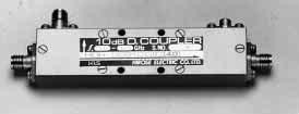
Figure 2: A directional coupler built based on a circuit-board stripline core is usually housed in a small, self-contained enclosure with discrete connectors; here, the Hirose HDH-00810GID(40) coupler shown is about 20 × 80 mm and has SMA-type connectors.
The MACP-009596-CA0160 from M/A-Com is an example of a directional coupler built with wirewound techniques (Figure 3). This broadband, 75 Ω coupler targets CATV applications and is specified for use between 5 and 1000 MHz. Despite the "wirewound", non-integrated construction, the PC-board footprint of this unit is just 3.8 × 4.0 mm (Figure 4).
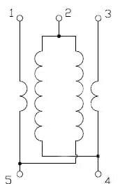
Figure 3: The wirewound MACP-009596-CA0160 directional coupler from M/A-Com is a broadband component for CATV applications, and handles 5 to 1000 MHz with a simple-transformer-like schematic.
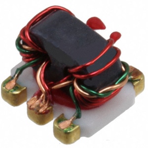
Figure 4: Despite the non-monolithic implementation of the MACP-009596-CA0160, it is not much larger than a SOT-6 IC.
Coupling loss is 10 dB over the specified frequency range, while transmission (mainline) loss ranges between 1.1 and 1.4 dB (typical) depending on where the measurement is made within the band, and between 1.4 to 1.7 dB (maximum). Similarly, directionality varies between 18 and 22 dB in band, with minimum values between 14 and 20 dB.
A monolithic, ceramic-based device, the DC4759J5020AHF directional coupler in the Xinger family from Anaren targets applications in the medium-width spectrum from 4700 to 5900 MHz such as the higher (5 GHz) Wi-Fi band, as well as point-to-point (P2P) and point-to-multipoint (P2MP) applications. The 50 Ω component is housed in a six-lead surface-mount package with a 1.3 × 2.0 mm footprint. Mean coupling from 4900 to 5500 MHz is 19.4 dB (typical); over the wider 4700 to 5900 MHz span, it is 19.7 dB (Figure 5). Insertion loss is 0.14 dB (typical) and 0.27 dB (maximum) over the narrower band, and 0.17 dB/0.32 dB (typical/maximum) over the range from 4700 to 5900 MHz.
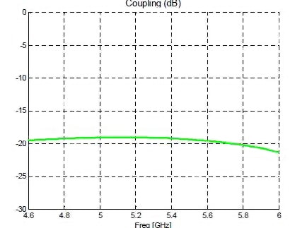
Figure 5: The flat insertion loss of the Anaren DC4759J5020AHF 20 dB coupler shows how it is a good fit for the 4700 to 5900 MHz band, now becoming increasing popular for newer-generation Wi-Fi due to more bandwidth and fewer interferers (such as microwave ovens and ISM users) compared to the crowded 2.4 GHz band.
The DC4759J5020AHF can also be used in designs which require a wideband front-end even though only a small slice of spectrum is of interest at a given time, such as multiband smartphones. For example, its insertion loss from 0 to 8500 MHz is under 0.4 dB over that entire frequency span (Figure 6). In this way, its insertion does not adversely affect users in cases where other signals of possible interest are far away from its narrower 4700 to 5900 MHz band of immediate interest.
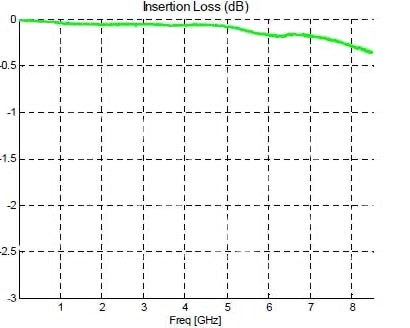
Figure 6: The key parameters of the DC4759J5020AHF are also provided for the 0 to 8500 MHz spectrum, making the IC a possible coupler in wideband systems; note that insertion loss is under 0.5 dB over that broad frequency range.
Summary
Although they do not directly add to the signal-processing chain's performance in an obvious way, directional couplers are an important part of the transmit feedback loop in many consumer products. By enabling the system processor and transmit-path management to better match power amplifier (PA) output to the specifics of the situation, they help achieve many goals: optimum use of transmit power, improvement in SNR at the receiver by carefully increasing output power if needed, operation within regulatory mandates, and longer battery run time.
For more information about the parts discussed in this article, use the links provided to access product pages on the DigiKey website.
聲明:各作者及/或論壇參與者於本網站所發表之意見、理念和觀點,概不反映 DigiKey 的意見、理念和觀點,亦非 DigiKey 的正式原則。


