Add High-Performance Speech Keyword Spotting to IoT Designs: Part 1 – Using FPGAs
資料提供者:DigiKey 北美編輯群
2018-09-27
Editor’s Note: Using an emerging class of efficient algorithms, any developer can now deploy sophisticated keyword spotting features on low-power, resource-constrained systems. Part one of this two-part series will show how to do it with FPGAs. Part two will show how to do it with MCUs.
Following the success of products that respond to a key phrase such as “Alexa,” “Hey Siri,” or “Hi Google,” keyword spotting (KWS) has become an important requirement for a growing array of embedded applications. While typical state-of-the-art KWS solutions rely on sophisticated convolutional neural networks (CNNs) and other deep neural network (DNN) machine learning algorithms, developers of resource-constrained products can get the accurate results they need using binarized neural networks (BNNs).
This article presents the benefits of adding KWS to wearables and other low-power IoT devices, before outlining the challenges. After describing the BNN architecture and why it’s a good approach for resource-constrained KWS applications, the article introduces an available solution that implements BNNs with low-power FPGAs. This solution will be used to show how to achieve the high accuracy of CNNs for low-power KWS implementations, at a fraction of CNNs’ resource requirements.
The origins and evolution of KWS
KWS, also known as key phrase detection, has for years found applications in information processing. In document processing, for example, KWS provides a more efficient alternative to optical character recognition for indexing large volumes of digitized documents. Speech-based KWS methods rapidly found attention in product development with the availability of voice activated services in smartphones, watches, home products, and others. In these products, an “always-on” feature allows the product to continuously process audio input, looking for the keyword designed to activate the voice-based user interface.
Board level products such as the XMOS VocalFusion 4-Mic Kit provide full integration with Amazon Voice Service, providing a ready solution for adding voice assistant services in many applications. For wearables or other battery operated products with limited power budgets, however, developers have largely been left to find their own KWS solutions.
Historically, implementing custom KWS mechanisms required developers to have significant background not only in audio engineering, but also in application of statistical methods for temporal pattern recognition. Statistical methods based on hidden Markov models and related algorithms have provided the basis for word spotting solutions for the past several decades.
More recently, DNN architectures such as the convolutional neural network (CNN) have begun to serve as the foundation for many KWS applications.
Addressing deep neural network (DNN) requirements
DNN architectures are based on multiple layers of neurons that are trained to extract features from input data and predict the probabilities that that input data corresponds to one of the classes used during training1. CNN architectures, in particular, have emerged as the preeminent approach for image recognition thanks to the high recognition accuracy achieved by these algorithms.
Similarly, different types of CNN architectures have found success in speech processing including KWS implementation. The difficulty with “conventional” CNN architectures has been their size and processing requirements. In image processing, for example, CNN models have grown to hundreds of megabytes in size. The combination of large memory size and extensive numerical calculation requirements places significant demands on the model processing platform.
The methods used to implement conventional CNN architectures offer little recourse. CNNs and other DNN algorithms achieve their accuracy through the use of general matrix multiply (GEMM) operations performed for each neuron at each layer in the network. During training, when models might need to process millions of labeled feature vectors to achieve desired results, the number of GEMM and other matrix calculations can easily number in the billions, driving the need for graphics processing units (GPUs) to speed processing in this phase of model development. When the model is deployed to perform inference in an application, the desire to maintain low latency and high accuracy continues to dictate a need for GPUs in the most demanding applications.
In applications with more modest inference requirements, developers can sacrifice latency and accuracy to deploy conventional CNNs even on general-purpose platforms like the Raspberry Pi Foundation Raspberry Pi 3, or Arm® Cortex®-M7-based MCUs such as those from Microchip Technology, NXP or STMicroelectronics2.
For applications that present strict requirements for inference accuracy and latency, however, conventional CNN algorithms are simply not practical on platforms with limited resources. CNNs present memory and processing requirements that lie well beyond the resources of an embedded system built into a typical line powered consumer product, much less a battery-powered wearable or other mobile design expected to offer “always-on” KWS capabilities. The development of model compression techniques has created a need for DNN algorithms able to support even these platforms.
Efficient DNN approaches
In an effort to address spiraling model sizes, machine learning scientists have found methods to dramatically reduce memory requirements with no significant loss in accuracy. For example, researchers pruned internal network connections that contributed little to the results. They also reduced the required precision of internal parameters down to 8-bit or even 5-bit values. Application of these and other methods reduce memory requirements by reducing the size of industry gold standard CNN models by 30x to 49x, with no appreciable loss in accuracy3.
Besides reducing memory requirements, model compression techniques also help reduce processing requirements: pruning reduces the number of required calculations, while precision reduction translates to faster calculations.
Even with their reduced precision, however, these networks still require a very large number of the GEMM operations that lie at the heart of machine learning algorithms. The extent of these operations not only drives the need for high-performance hardware in inference platforms, but also directly impacts the power budget of those platforms. The power consumed just for the very high number of memory accesses required to feed these matrix operations can by itself easily exceed the power budget of battery-powered devices.
To address memory, processing, and power limitations of mobile devices, researchers have extended the notion of model compression to its extreme. Rather than simply reducing the precision of internal parameters to eight or fewer bits, researchers have quantized model parameters down to values of +1 or -1 (or 0) to create an architecture called a binarized neural network (BNN).
How BNNs bring KWS to resource-limited designs
In terms of basic topology, BNNs appear largely the same as CNNs and include the same kind of layers including convolution, normalization, activation, and pooling. The use of 1-bit parameters (weights and bias values) within those layers provides a profound difference in operation.
Rather than performing 32-bit floating-point GEMM operations required in conventional CNNs, BNNs can use simpler bitwise XNOR operations. Although this approach can result in longer training time, researchers have found that BNN models achieve nearly the accuracy rates as models using 32-bit floating-point values4. The use of binarized parameters not only reduces the memory footprint of BNNs, but also reduces their memory access requirements because multiple 1-bit parameters can be fetched in a single word access cycle, and fewer of those are needed to feed the XNOR operations.
BNN's simpler calculations also translate to a dramatic reduction in processing requirements. As a result, BNNs can achieve higher inference rates than earlier methods without significantly compromising accuracy. In one study, researchers compared the performance of a CNN and a BNN implemented on a Xilinx XC7Z020 FPGA system-on-chip (SoC) running on an XC7Z020-based development platform such as Digilent’s ZedBoard. Using the XC7Z020 FPGA, both DNNs offered highly efficient performance, but the CNN achieved about 7.27 giga operations per second (GOPS) per watt, while the BNN delivered 44.2 GOPS/watt on the same part5.
Due to their programmability and high efficiency, FPGAs have emerged as a popular inference platform for applications such as embedded vision using CNNs6. Advanced FPGAs offer a combination of embedded memory, and multiple parallel processing digital signal processing (DSP) units needed to speed GEMM and other matrix calculations. Although BNNs require a fraction of the DSP resources required for CNNs, FPGAs remain well suited to these architectures as well. For example, developers can enhance their FPGA-based BNNs with specialized logic able to speed binary convolutions or other bitwise operations used in this architecture.
For the typical developer focused on the larger application, however, designing any type of optimized FPGA-based DNN can introduce delays even as project schedules shrink to pace fast moving application areas like wearables and other voice activated connected products. The SensAI™ technology stack from Lattice Semiconductor eliminates this obstacle with specialized DNN IP, reference designs, design services, and a simple FPGA development workflow for implementing inference models.
FPGA-based BNN solution
SensAI combines DNN IP with a neural network compiler in a work flow designed to speed implementation of neural network models created with industry standard machine learning frameworks including Caffe and TensorFlow (Figure 1).
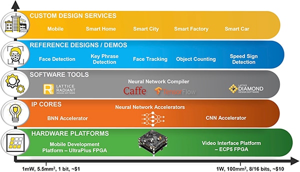
Figure 1: The Lattice SensAI technology stack helps developers use CNN and BNN models created with standard machine learning frameworks to implement low-power inference engines on Lattice iCE40 UltraPlus and ECP5 FPGAs. (Image source: Lattice Semiconductor)
Designed for use with Lattice ECP5 FPGAs, Lattice's CNN IP does support high-performance image recognition at 1 W or less running on Lattice's ECP5-based Embedded Vision Development Kit. However, for resource-constrained designs, Lattice's BNN IP lets developers take full advantage of this efficient architecture to implement inference engines on low-power Lattice ICE40 UltraPlus FPGAs.
Using the Lattice BNN IP, these ICE40 UltraPlus-based inference engines achieve high accuracy while operating at significantly lower power, using fewer memory and processing resources. Lattice demonstrates the efficiency of this BNN IP in a complete ICE40 UltraPlus FPGA implementation of a KWS inference model that consumes about 1 mW while running on the Lattice Mobile Development Platform (MDP).
The Lattice SensAI BNN IP includes a full complement of modules required to implement a BNN inference solution (Figure 2).
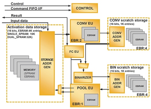
Figure 2: Lattice SensAI IP provides a full set of model layers, memory subsystems, control logic, and system interfaces needed to implement a BNN solution on a Lattice iCE40 UltraPlus FPGA. (Image source: Lattice Semiconductor)
Along with support for convolution, pooling, and other DNN layer functionality, the IP includes multiple memory subsystems including those for the model's fixed parameters developed during training and for intermediate results from calculations performed during inference. Along with interface logic for input, output, and control lines, the IP provides a control subsystem used to process the command sequences that implement model operations.
For a new project, developers use a few simple menus in the Lattice Radiant software package to generate the basic IP core for their particular design. Here, developers simply configure the BNN IP block for the desired memory (8, 16, or 64 Kbytes) and binary type (either +1/–1 or +1/0) using menu options presented in the Radiant IP configuration wizard. Developers complete this simple setup procedure by using another Radiant menu to generate the RTL and other support files used by the Radiant FPGA programmer to program the device with their selected BNN configuration.
While this FPGA programming workflow provides the underlying execution platform for BNN models, the programming of the model itself follows a separate path in the SensAI environment.
In the model development portion of the SensAI workflow, developers use the Lattice Neural Network Compiler to convert Caffe or TensorFlow models into files containing the model parameters and command sequences needed to implement those models on the configured BNN core. In the final step, developers use Radiant to load the model files and FPGA bitstream files into the FPGA platform.
KWS implementation
Lattice demonstrates this BNN development process with a complete BNN-based KWS model designed to operate on the Lattice MDP. The MDP offers a compelling platform in its own right, combining iCE40 UltraPlus FPGAs with a broad set of peripherals likely to be encountered in a typical low-power mobile application.
The board integrates four iCE40 UltraPlus devices, each showcased in applications demonstrating the board's built-in 1.54 inch display, 640 x 480 image sensor, and RGB LED. The board also includes a full set of sensors including pressure, compass, 3-axis linear accelerometer, and 3D accelerometer and 3D gyroscope. For audio applications such as keyword detection, the board includes two I2S microphones and two PDM microphones. For more demanding applications, developers can plug Lattice's 8 microphone LF-81AGG-EVN daughter board into the MDP to support audio beamforming for enhanced directional response in their voice activated applications (Figure 3).
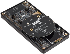
Figure 3: The Lattice Mobile Development Platform (MDP) integrates an extensive set of support features and peripherals while providing connectors for add-ons such as the 8 microphone array (shown attached to the MDP). (Image source: Lattice Semiconductor)
The board's built-in power management circuit allows developers to power the board from its internal Li-ion battery for standalone operation or from an external source. During development, the board can be powered through its USB connection to a host development platform. This host can be running Lattice iCEcube2 for creating custom designs, or running the Lattice Radiant Programmer to program the onboard iCE40 FPGAs with prebuilt designs such as the Lattice key phrase detection demo.
Lattice DNN demos, including one for keyword phrase detection, provide a complete set of files normally generated through the SensAI workflow. As such, developers can simply load those files using the Radiant Programmer to evaluate performance of models such as the BNN inference model featured in the keyword phrase detection demo.
For developers looking to examine implementation details, the demo projects also provide model files including a TensorFlow .pb file and Caffe .proto and .caffeemodel files. Developers can inspect these models to evaluate the provided network design. For applications with more specialized requirements, these models can be used as the starting point for developers’ own models. Typically, designers will find topologies based around typical CNN type designs.
In the Lattice key phrase detection demonstration project, the supplied BNN network design uses a familiar topology, repeating multiple stages that each comprise convolution, batchnorm normalization, scaling, ReLu activation, and pooling layers (Figure 4). Although largely indistinguishable from a conventional CNN design, the Lattice BNN implementation features the internal binarized parameters and associated mechanisms at the heart of this highly efficient architecture.

Figure 4: Included in a Lattice demonstration project, a BNN performs key phrase detection using a pipeline of three similar convolution modules, each comprising a convolution layer, batchnorm normalization, scaling, ReLU activation, and pooling. (Image source: Lattice/Ethereon)
The Lattice demo implements this BNN inference model as a BNN accelerator engine embedded in the FPGA with modules for managing the audio stream and command sequence loaded from external flash (Figure 5).
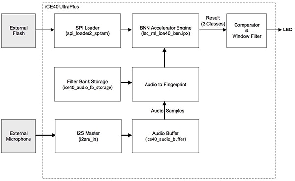
Figure 5: The Lattice key phrase detection demo implements a complete KWS system on a single low-power Lattice iCE40 UltraPlus FPGA. (Image source: Lattice Semiconductor)
Here, the I2S master block accepts audio data from the external microphones and passes the data to the audio buffer. In turn, the audio-to-fingerprint block reads audio samples from the buffer and uses filters that are read from filter bank storage to generate a basic audio spectrogram. This provides a suitable result without the computational complexity of a traditional FFT spectrogram.
Finally, the BNN accelerator engine uses this processed audio stream for inference, producing three possible outputs: silence, key phrase, no key phrase.
After the board is configured and the demo files are loaded, developers can run the demo simply by applying power to the MDP board and speaking the key phrase (in this case, the word “seven”). When the inference engine detects the key phrase, the FPGA turns on the RGB LED built into the MDP.
Conclusion
Machine learning provides a powerful solution for enhancing wearables and other mobile applications with powerful features such as keyword spotting used with voice activated user interfaces. Although machine learning model architectures such as CNNs can provide highly accurate results, their requirements for memory, processing, and power typically exceed the resources of battery-operated devices.
As shown, the BNN architecture addresses these concerns, and using an advanced machine learning solution from Lattice Semiconductor, developers can rapidly augment their designs with KWS capabilities while consuming approximately 1 mW.
References:
- Getting started with machine learning for the IoT, DigiKey
- Build a Machine Learning Application with Raspberry Pi, DigiKey
- Deep Compression: Compressing Deep Neural Networks with Pruning, Trained Quantization and Huffman Coding
- Binarized Neural Networks: Training Deep Neural Networks with Weights and Activations Constrained to +1 or -1
- Accelerating Binarized Convolutional Neural Networks with Software-Programmable FPGAs
- Use FPGAs to Build High-Performance Embedded Vision Applications with Machine Learning, DigiKey

聲明:各作者及/或論壇參與者於本網站所發表之意見、理念和觀點,概不反映 DigiKey 的意見、理念和觀點,亦非 DigiKey 的正式原則。


