Virtual Antennas Simplify IoT Embedded Antenna Design
Antennas have always existed in a contradictory and sometimes confusing place in the wireless world. On one side, they are just simple passive transducers between the confined energy in conductors as represented by voltage and current, and the dispersed, radiating electromagnetic energy existing in a vacuum or air. On the other side, they are available in a bewildering range of physical embodiments, configurations, styles, and sizes. Since the earliest days of wireless (think Marconi and over a century ago), the conception, design, and fabrication of antennas has gone through several major phases.
The first phase
The first antennas were based on one of two fundamental structures: the monopole with an associated ground plane (sometimes called a whip antenna) (Figure 1), and the balanced, ungrounded dipole in various configurations such as the folded dipole (Figure 2). While researchers and engineers knew that antenna performance was ultimately governed by Maxwell’s four crisp equations, making use of these equations for antenna design was not possible due to the enormous complexities involved in modeling and computation.
 Figure 1: The long wire or whip antenna arrangement is a single-element design using a ground plane (here, the car’s surface) (left); the illustration of the antenna shows its simplicity (right). (Image sources: Lihong Electronic (left); Electronics Notes (right))
 Figure 2: The basic dipole is a balanced, symmetrical antenna without a ground reference (top), as shown in the illustration (bottom). (Image sources: TCARES.net (top) and Tutorials Point (bottom))
As a result, antenna-related analysis was limited to basic equations which were used to size the elements of antennas such as the monopole, dipole, long wire, and a few other configurations. These equations were also modified using rules of thumb, intuition, and field trials. For example, it was known that using tubing rather than thin wires for dipoles increased their bandwidth, which might be good or bad depending on the application; the amount of this increase versus tubing diameter was estimated using guidelines based on experience and basic measurements. Even academic discussions of antenna designs and their operating principles had few equations beyond basic arrangement versus wavelength discussions, as made clear in the 1926 technical paper for the classic Yagi-Uda antenna (Reference 1) (Figure 3).
 Figure 3: The basic Yagi antenna (top) is a three-element antenna widely used in commercial, residential, and military applications. The three elements (bottom) are a driven (active) dipole element with a passive reflector behind it and a passive director in front of it, all mounted on a single boom. (Image sources: EuroCaster/Denmark (top); RFWireless-World (bottom))
The second phase
The second wave of antenna-design innovation began with the availability of models and algorithms that captured antenna attributes, which could be executed on computers to solve the electromagnetic field models and equations in a reasonable amount of time, as long as the models were not too complicated.
These “field solvers” allowed designers of new antenna configurations to use the combination of antenna theory and field-experience insight to propose new arrangements, model them, and finally quantify their performance “on paper”, without need for a physical model and field tests in their initial design stages. This approach worked to some extent, but it was still somewhat of a hit-or-miss arrangement. It did, however, enable engineers to focus on an antenna design and iteratively adjust and tweak it until it met the project objectives.
An extraordinary example of this was seen in the development of the first stealth aircraft, the F-117 Nighthawk, at Lockheed’s legendary Skunk Works (References 2 and 3). Much the of theoretical work on reducing its radar signature by many orders of magnitude was based on analytical solutions and complex equations.
These equations analyzed the reflection of electromagnetic energy fields on the aircraft as it was bathed in radar signals. The project’s objective was to use unique and unconventional choices in skin-panel material, shape, size, angles, joints, and other design elements to minimize the inherent tendency of these surfaces to act as an antenna. This, in turn, caused the aircraft to re-radiate and reflect energy in an antenna-like mode, and thus be invisible to the radar system receiver.
Third phase is very different
We are now entering a new wave of model-based antenna design, one which looks at the challenge from a different perspective. Instead of relying on a dedicated antenna to radiate an RF signal, the Internet of Things (IoT) device or smartphone radiates the signal directly from the ground plane.
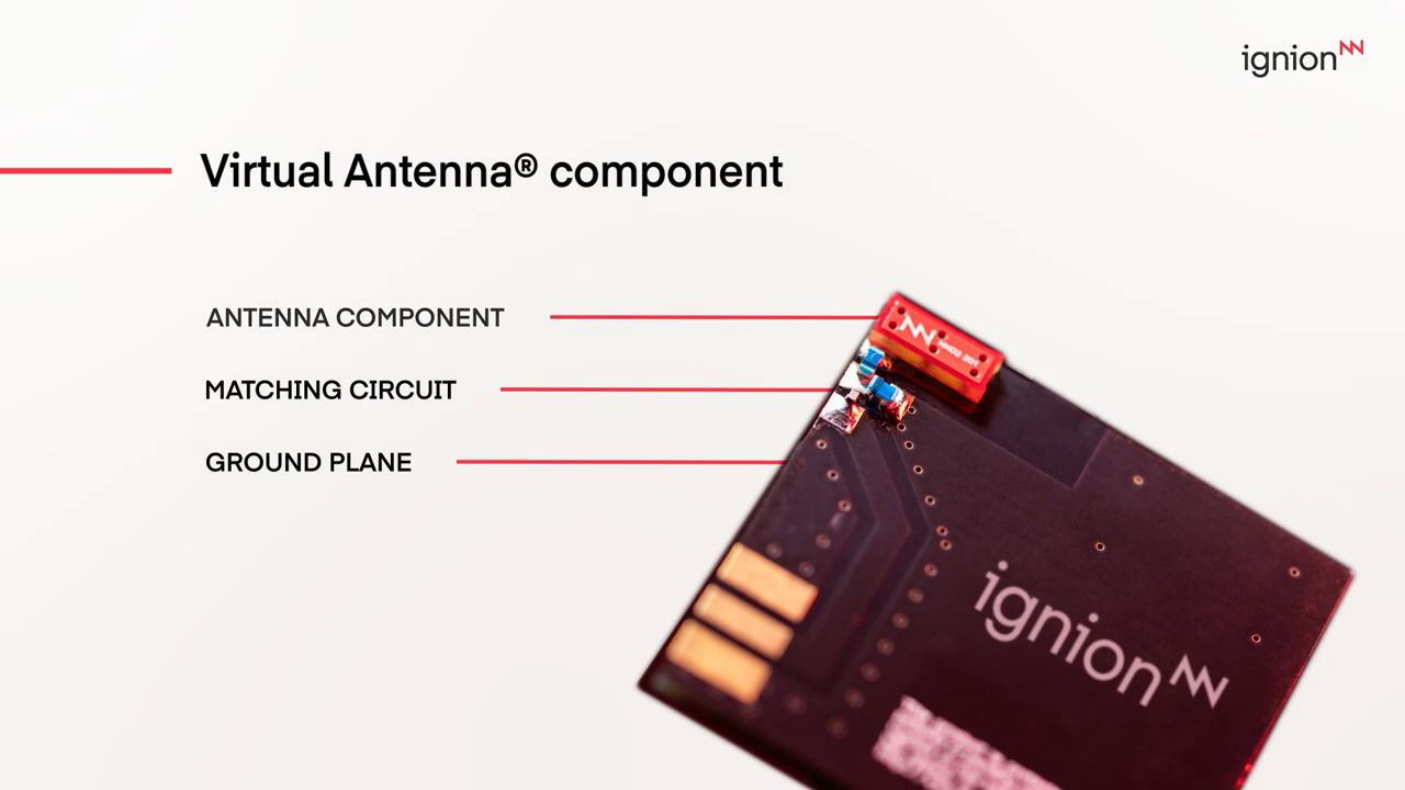
To do this, a conventional embedded antenna is replaced with an Ignion NN03-320 DUO mXTEND antenna booster (Figure 3), a 7.0 millimeter (mm) long × 3.0 mm wide × 2.0 mm high passive component that is roughly one-tenth the size of a traditional antenna (note that Ignion was known as Fractus Antennas until 2021).
 Figure 4: The Ignion NN03-320 DUO mXTEND is a tiny passive component that uses a product’s circuit board ground plane to radiate the RF signal. (Image source: Ignion)
With its unique and patented Virtual Antenna technology—the commercial name for the "antenna-less" technology based on a new generation of tiny components—this booster is always the same component regardless of the size or form factor of the printed circuit board. The designer tunes it to the desired frequency band(s) by creating and adjusting the matching network’s component arrangement and values.
In other words, this arrangement creates a new and beneficial synergy between the antenna booster and the surrounding ground plane. A rough analogy would be the effect of attaching a small audio-piezo driver to a rigid tabletop: the tabletop would resonate and, in effect, significantly boost the resultant audio output level.
The Ignion antenna boosters are standard, off-the-shelf, surface-mount components that replace conventional customized planar inverted-F antennas (PIFAs) and printed-circuit antennas. They are much smaller than the operating wavelength, typically below 1/30 or even 1/50 of the wavelength and beyond. They provide fully functional multiband wireless connectivity, enabling a single antenna booster component to function effectively across multiple mobile and wireless designs, thus reducing time to market, product development investments, and of course, cost. In addition, as the antenna boosters are physically built as chip antennas, they can be installed using conventional pick-and-place systems, resulting in lower production cost and improved quality and reliability.
Making a match
The matching network is key to realizing the unique booster performance. While the antenna booster is standard and can be used across a variety of mobile products, the matching network does need customization for every product, but this is a one-time, up-front design effort.
By changing the matching network, the booster’s RF response can be customized to cover the multiple frequency bands required in a modern IoT device or smartphone. The simpler single-band IoT device needs a matching network with typically three to five components, while a multiband smartphone might need a couple of boosters and five to eight high-Q components for its matching network.
Ignion simplifies the design effort with a free development tool which lets the designer virtually place the booster near the edge of the circuit board, define a “clear” zone around the booster devoid of components, and then calculate the needed passive comments for the matching network. For the multiport NN03-320, the calculated matching networks allow the device to cover multiple bands and applications including GNSS, Bluetooth, 5G and UWB, over frequencies spanning 1561 to 1606 megahertz (MHz), 2400 to 2500 MHz, 3400 to 3800 MHz, 3100 to 4800 MHz, and 6 to 10.6 gigahertz (GHz) (Figure 5).
 Figure 5: The NN03-320 antenna booster can be used for different and/or multiple bands when fitted with the suitable passive component matching circuit between the RF source and the booster. (Image source: Ignion)
The NN03-320 datasheet specifies the performance of this 50 ohm (Ω) Virtual Antenna booster component and optimized matching network using standard antenna parameters for each band, including efficiency, peak gain, VSWR, polarization, and radiation pattern.
Application notes show typical matching network schematic diagrams like Figure 6, and include a table of suggested passive component values for each desired frequency span. While these values serve as starting points, they will need to be tweaked to account for unanticipated parasitics, as well as the effects of nearby components such as displays or ICs.
 Figure 6: This suggested schematic diagram for a dual-band matching network also comes with a table of suggested passive component values to provide a starting point for design, analysis, and evaluation. (Image source: Ignion)
Conclusion
Antenna boosters such as these from Ignion represent a different way of radiating RF energy by using the ground plane as a radiating surface. These passive, surface-mount booster devices offer an alternative to conventional embedded antenna arrangements for IoT devices and smartphones. A single Virtual Antenna device can serve different parts of the RF spectrum, simply by appropriate configuration of its passive matching network.
References
1: Yagi, Hidetsu; Uda, Shintaro, Proceedings of the Imperial Academy (February 1926). "Projector of the Sharpest Beam of Electric Waves" (PDF).
2: Air Force Magazine, “How the Skunk Works Fielded Stealth”
3: Ben Rich, “Skunk Works: A Personal Memoir of My Years of Lockheed”
About this author

Bill Schweber is an electronics engineer who has written three textbooks on electronic communications systems, as well as hundreds of technical articles, opinion columns, and product features. In past roles, he worked as a technical web-site manager for multiple topic-specific sites for EE Times, as well as both the Executive Editor and Analog Editor at EDN.
At Analog Devices, Inc. (a leading vendor of analog and mixed-signal ICs), Bill was in marketing communications (public relations); as a result, he has been on both sides of the technical PR function, presenting company products, stories, and messages to the media and also as the recipient of these.
Prior to the MarCom role at Analog, Bill was associate editor of their respected technical journal, and also worked in their product marketing and applications engineering groups. Before those roles, Bill was at Instron Corp., doing hands-on analog- and power-circuit design and systems integration for materials-testing machine controls.
He has an MSEE (Univ. of Mass) and BSEE (Columbia Univ.), is a Registered Professional Engineer, and holds an Advanced Class amateur radio license. Bill has also planned, written, and presented on-line courses on a variety of engineering topics, including MOSFET basics, ADC selection, and driving LEDs.

Have questions or comments? Continue the conversation on TechForum, DigiKey's online community and technical resource.
Visit TechForumRelated Blogs


More Blogs from this Author