Power Multiple Semiconductor Devices Using a Single Multichannel DC/DC Converter
Contributed By Electronic Products
2015-10-27
To perform multiple tasks from a single board, modern system boards are populated with a variety of semiconductor devices including DSPs, microprocessors, ASICs, FPGAs, memory, and more. Typically, these semiconductor ICs are fabricated using sub-micrometer processes, and therefore require low supply voltages to operate. Because of this, these boards employ an intermediate bus architecture to step-down high bus voltage like 48 VDC to 12 VDC, 9.6 VDC, or 5.0 VDC. This lower intermediate bus voltage is then used to power a number of dedicated and efficient point-of-load (POL) regulators or step-down DC/DC converters that further generate the required 3.3 V (and lower) voltages for powering these semiconductor devices. As a result, the boards are packed with several POL regulators and DC/DC buck converters.
However, using multiple switching POL regulators and buck converters translates into higher cost, lower overall efficiency, and more board space. So it should not be surprising that designers facing space constraints are looking for an integrated solution which generates multiple regulated low-output voltages from a single, synchronous step-down DC/DC converter package. Suppliers addressing such needs include Linear Technology and Texas Instruments (TI) to name just two.
To extend the possible range of applications for their new solutions, these suppliers are broadening their product portfolios, offering new members with better performance, novel features, and configurable outputs. This article will examine these new multichannel synchronous buck DC/DC converters in detail. Besides uncovering their performance and characteristics, we will also reveal a new multi-output configurable step-down DC/DC converter that incorporates digital control (or programmable pins) to further simplify the buck-converter configuration process.
Multichannel buck converters
Speaking of new members, TI has unveiled a four-channel synchronous buck converter with digital PMBus/I2C interface. Designed to run from an intermediate-distribution bus voltage, TPS65400 offers four high-current buck-switching regulators (SW1, SW2, SW3, and SW4) with integrated FETs. Each switching converter is capable of supplying a 2 A or 4 A output to efficiently power semiconductor ICs such as a microprocessor, FPGA, ASIC, memory, and digital input/output (Figure 1). As per Figure 1, SW1 and SW2 support 4 A each, and SW3 and SW4 support 2 A each. The input-voltage range for the converter is 4.5 V to 18.0 V, supporting applications running off a 12 V or 5 V intermediate bus. Also, the multichannel buck converter’s switching frequency can be independently adjusted up to 2.2 MHz.

Figure 1: TI’s TPS65400 is a multichannel synchronous buck converter that offers four high-current synchronous buck-switching regulators with integrated MOSFETs. Each switching converter supplies a 2 A or 4 A output to efficiently power myriad digital ICs.
According to TI, the multichannel buck is designed to offer both internal and external sequencing of the four integrated buck-switching regulators. As per the description in the product data sheet, sequencing requirements can be met using the individual enable pins or by programming the sequence through the I2C bus into the onboard EEPROM. Detailed descriptions are given in the TPS65400 data sheet. Output voltages can be set through external resistor networks and VREF can be programmed from 0.6 to 1.87 V in 10 mV steps. All control and status information can be accessed through a PMBus-compatible I2C bus.
Applications for the part include small cellular base stations, Power over Ethernet (PoE) powered communications infrastructure equipment and automotive infotainment and telematics.
For applications needing a smaller footprint and higher efficiency, TI has released integrated triple-output synchronous buck converters in QFN packages with up to 96 percent efficiency. Offering a 44 percent smaller footprint than previous-generation parts, triple-output buck converters TPS65261 (Figure 2) and TPS65262 feature wide-input-voltage range of 4.5 V to 18 V with integrated automatic power up/down for easy power control. While TPS65261 offers output currents of 3 A/2 A/2 A, TPS65262 is rated to deliver output currents of 3 A/1 A/1 A.

Figure 2: TPS65261 is an integrated triple-output synchronous buck converter with a wide-input-voltage range of 4.5 V to 18 V. Maximum continuous output current is rated at 3 A/2 A/2 A.
The switching frequency of the converters can be adjusted from 250 kHz to 2 MHz with an external resistor. The 180° out-of-phase operation between Buck1 and Buck2, Buck3 (Buck2 and Buck3 run in phase) minimizes the input-filter requirements, says the maker. The data sheet indicates that the feedback voltage reference for each buck regulator is 0.6 V. Furthermore, the functional block diagram of TPS65261 suggests that each buck converter is independent with dedicated enable, soft-start, and loop compensation pins. Applications include digital TV, set-top boxes, home gateways, and wireless routers.
For lower-power FPGAs, DSPs, and microprocessors, TI offers the quad-output step-down converter LP8728-Q1. It packs four highly efficient step-down DC/DC converters into one WQFN package, as illustrated in Figure 3. Each converter has high-current capability and separate controls which allows flexibility to use the device in multiple applications. Also, each converter’s output voltage is fixed. LP8728-Q1’s data sheet shows that the output voltage for Buck1 (VOUT1) is 3.3 V and Buck2 (VOUT2) is 1.25 V. Likewise, output voltage for Buck3 (VOUT3) is 1.8 V or 2.65 (pin selectable) while Buck4 (VOUT4) offers 1.8 V. Maximum output current for the quad-output buck converter is 1 A.

Figure 3: TI’s LP8728-Q1 packs four highly efficient step-down DC/DC converters into one WQFN package.
All the converters operate with a fixed 3.2 MHz switching frequency and utilize 1.5 μH inductors, recommended by the manufacturer. Because DC resistance of the inductor directly impacts the efficiency of the buck converter, it is important to use inductors with the lowest possible DC resistance for achieving highest efficiency. In addition, the product’s data sheet suggests using inductors with saturation-current rating equal to or higher than the high-side switch current limit (1500 mA). Selection of other external components like input/output capacitors is also discussed in the quad-output step-down DC/DC converter’s data sheet.
Configurable regulators
Linear Technology’s LTM4644 is a quad-output step-down μModule regulator that is configurable as single-, dual-, triple-, or quad-output regulator. This flexibility enables system designers to replace multiple POL regulators and DC/DC converters with a single multi-output device1. This year the company has expanded the line with new members. The latest configurable addition is LTC3371, a four-channel configurable buck DC/DC with independent input for each buck converter (Figure 4). Encased in a thermally enhanced 38-lead QFN package, it can be configured to share eight 1 A power stages, each of which is powered from independent 2.25 to 5.5 V inputs. Applications include general-purpose multichannel power supplies, automotive-, industrial-, and distributed-power systems.

Figure 4: Linear’s LTC3371 is a four-channel configurable buck DC/DC converter that can be configured to share eight 1 A power stages, each of which is powered from independent 2.25 to 5.5 V inputs.
Using programmable pins C1 – C3, the Buck1, Buck2, Buck3, and Buck4 DC/DC converters can be configured for outputs from 1 A to 4 A with maximum output of 8 A as illustrated in Table 1. Also, it can be configured to deliver dual, triple, or quad outputs. The common buck-switching frequency may be programmed with an external resistor, synchronized to an external oscillator, or set to a default internal 2 MHz clock.
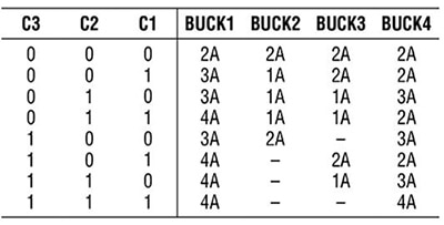
Table 1: Each buck converter of LTC3371 can be configured to offer eight unique outputs using pins C1 – C3.
In summary, suppliers are constantly adding new members to their single multichannel step-down DC/DC converter families, giving designers more choices for their end applications. With broader specs and more features, including configurable outputs, these integrated multichannel buck converters are addressing a wide range of applications.
For more information on the parts discussed in this article, use the links provided to access product pages on the DigiKey website.
References
- “Configurable 4-in-1 Regulator Powers FPGAs, ASICs and Microprocessors” by Ashok Bindra, Electronic Products, September 9, 2014.
Disclaimer: The opinions, beliefs, and viewpoints expressed by the various authors and/or forum participants on this website do not necessarily reflect the opinions, beliefs, and viewpoints of DigiKey or official policies of DigiKey.