Optimize SMPS Efficiency with a Multi-Technology Approach
Contributed By DigiKey's North American Editors
2025-09-17
The efficiency and robustness of switch-mode power supplies (SMPSs) make them suitable for applications such as electric vehicle (EV) charging infrastructure, solar inverters, and industrial motor drives. However, the demand for higher operating voltages and currents, reduced conduction and thermal losses, and more compact form factors requires designers to incorporate advanced silicon carbide (SiC) MOSFET technology. This technology must be combined carefully with MOS-gated thyristors and fast-recovery bridge rectifiers to produce the optimal power conversion system.
This article provides an overview of SMPS requirements using an EV charger example. It then introduces SiC MOSFETs from IXYS/Littelfuse, examines their capabilities, and demonstrates how combining different device technologies, each optimized for specific circuit functions, creates more efficient and compact power conversion systems.
Overview of modern SMPS using a public fast EV charger infrastructure as an example
Efficiency is a signature SMPS characteristic, but modern high-power applications are pushing these designs to new extremes. Consider the requirements of a public direct current (DC) fast charger, such as a Level 3 system delivering up to 350 kW. A 1% loss in efficiency translates to 3.5 kW of wasted power, significantly increasing both the operating cost and the thermal load.
High-performance SiC MOSFETs are central to achieving greater efficiency. Their ability to switch at high frequency while maintaining low conduction resistance enables smaller passives and reduces conversion losses. Unfortunately, these same factors make SiC MOSFETs vulnerable to transient voltage surges. Therefore, high-efficiency designs typically require more advanced protection schemes.
Also, SiC MOSFETs are not the best solution for every part of a Level 3 charger. For example, public chargers require an auxiliary power system for coolant pumps, network communications, and other system functions. These systems must remain operational even if the primary charging path is interrupted. Here, a high-reliability silicon (Si) diode-based device may be a better choice.
It is essential to understand the requirements of each section of a DC fast-charging station and carefully choose the appropriate device technology.
Using low-resistance SiC MOSFETs for high-power DC-DC conversion
The DC-DC conversion stage of a Level 3 fast charger illustrates the challenges of modern SMPS design. With output voltages up to 1 kilovolt (kV), this stage traditionally required either high-voltage Si insulated gate bipolar transistors (IGBTs) or the use of a high-voltage SiC MOSFET. Both approaches could introduce efficiency penalties: IGBTs through high switching losses and, in the case of some early-generation SiC MOSFETs, through relatively high conduction losses. For example, some early-generation high-voltage SiC MOSFETs had an on-state resistance (RDS(ON)) in the realm of 100 mΩ.
The Littelfuse IXSJxxN120R1 SiC MOSFET family offers a compelling solution to this dilemma. This family combines a blocking voltage up to 1200 volts with an RDS(ON) as low as 18 mΩ. This low resistance minimizes conduction losses and provides superior thermal performance.
The devices are packaged in an isolated ceramic package with 2,500 VAC isolation (1 minute). This design lowers junction-to-heatsink thermal resistance and reduces electromagnetic interference (EMI) by minimizing stray capacitance to the heatsink, while using the familiar TO-247-3L package for ease of integration.
A typical example is the IXSJ43N120R1 (Figure 1). This device is rated for a continuous drain current ID of 45 A at +25°C, with an RDS(ON) of 36 mΩ (typical). It also offers a low gate charge of 79 nC and an input capacitance of 2453 pF, lending itself to designs with smaller magnetics.
 Figure 1: The IXSJ43N120R1 1,200 V SiC MOSFET comes in an isolated TO-247-3L package and is rated for a continuous drain current ID of 45 A at +25°C, with an RDS(ON) of 36 mΩ (typical). (Image source: Littelfuse)
By reducing conduction losses while maintaining high-voltage blocking capability, the IXSJxxN120R1 family enables designers to simplify converter topologies, reduce thermal overhead, and maximize overall system efficiency.
Minimizing switching losses in active front-end performance
In other parts of a DC fast charger, switching losses can be more critical than conduction resistance. Consider the active front-end, which converts AC to DC while shaping the current waveform to meet power factor correction (PFC) and harmonic distortion requirements. Because this stage relies on elevated switching frequencies to minimize inductor and filter size, switching losses play a significant role in the overall efficiency.
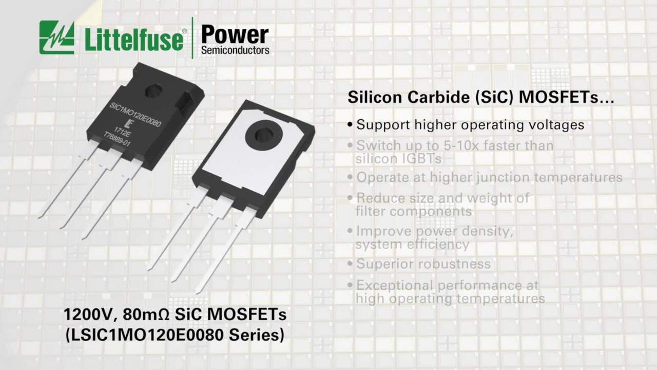
The LSIC1MO120E SiC MOSFET series from Littelfuse is optimized for these high-frequency applications. These devices combine 1200 volt blocking capability with low dynamic losses, making them well-suited to PFC boost converters in DC fast chargers and other grid-connected systems.
For example, the LSIC1MO120E0080 (Figure 2) is rated for a continuous drain current (ID) of 39 A at +25°C, and it balances a respectable RDS(ON) of 80 mΩ (typical) with a low switching energy per cycle of 252 µJ. An extended junction temperature range of -55°C to +175°C provides additional design margin in outdoor installations where ambient conditions vary widely.
 Figure 2: The LSIC1MO120E0080 SiC MOSFET is optimized for high-frequency applications. (Image source: Littelfuse)
The LSIC1MO120E series comes in a non-isolated TO-247-3 package. By pairing the switching loss-optimized LSIC1MO120E in the front-end with the conduction loss-optimized IXSJxxN120R1 in the DC/DC stage, designers can optimize efficiency across the entire fast-charging power chain.
Advanced circuit protection with MOS-gated thyristors
To ensure reliable operation, DC fast-charging systems must withstand grid-induced surges as well as sudden energy discharges from the DC link during faults. Crowbar-style protectors are often used to guard sensitive systems from these hazards, but as power levels rise, these protection systems need higher current handling capability and faster response times. A MOS-gated thyristor such as the MMIX1H60N150V1 (Figure 3) in a 24-SMPD package is an excellent fit for these requirements.
 Figure 3: The MMIX1H60N150V1 MOS-gated thyristor comes in a 24-SMPD package. (Image source: IXYS/Littelfuse)
Three attributes stand out for use in DC charger crowbar circuits:
- High surge capability: Rated at 32 kiloamperes (kA) for 1 microsecond (µs) and 11.8 kA at 10 µs, the device can absorb severe disturbances without compromising downstream SiC MOSFET stages.
- Fast triggering characteristics: A 50 nanosecond (ns) delay and a 100 ns current rise time support rapid clamping of overvoltage events before they propagate into the converter.
- Integrated anti-parallel diode: This feature allows the device to handle bidirectional fault currents, an important safeguard against DC link disturbances.
Together, these attributes make the MMIX1H60N150V1 a robust choice for protecting high-power DC fast-charging systems.
Ensuring system availability and auxiliary power with bridge rectifiers
Beyond the primary power path, public DC fast chargers require auxiliary power for systems such as cooling pumps, payment terminals, displays, and communication links. The VBE60-06A bridge rectifier (Figure 4) is designed to provide the high availability demanded by these critical functions.
 Figure 4: The VBE60-06A bridge rectifier provides screw holes for easy mounting. (Image source: IXYS/Littelfuse)
Built on high-performance, fast recovery diode (HiPerFRED) technology, the VBE60-06A combines low conduction loss with soft reverse recovery characteristics. Three attributes in particular support its use in demanding infrastructure applications:
- High power capacity: With a 600 volt reverse blocking voltage and a 60 A bridge output current, the device provides ample margin for derating in outdoor equipment that must operate continuously across a wide temperature range.
- Low EMI: A reverse recovery time of only 35 ns, combined with soft recovery behavior, minimizes switching losses and reduces the high-frequency emissions that can cause EMI. Minimizing EMI is critical in systems integrating sensitive communications and control electronics.
- Robust operation: The rectifier is avalanche-rated for reliable performance under transient conditions. Its industry-standard SOT-227B minibloc package provides 3000 volts isolation, improving system safety and simplifying integration into high-voltage assemblies.
By delivering reliable and electromagnetically quiet rectified power for auxiliary subsystems, the VBE60-06A supports the uptime and availability targets that are essential to public charging networks.
Designing complete system solutions for SMPS applications
The system-level design principles discussed for EV fast chargers are directly applicable to other demanding SMPS applications. In solar inverters, for example, maximizing energy harvesting depends on minimizing both conduction and switching losses in the maximum power point tracking (MPPT) and inverter stages. Using the appropriate SiC MOSFETs in concert can achieve both goals, while robust surge protection with MOS-gated thyristors can safeguard system longevity and uptime.
Industrial motor drives present similar challenges. High-frequency switching enables precise motor control while reducing vibration, but it also increases thermal stress. Low-loss SiC MOSFETs help control these demands, improving efficiency and lowering operating costs. At the same time, electrically harsh industrial environments call for the fast-acting, high-current protection that MOS-gated thyristors provide, ensuring the reliability required in continuous industrial operations.
Furthermore, both solar inverters and industrial motor drives employ auxiliary power for control, monitoring, and other critical systems. These functions require a dependable and electromagnetically quiet power source, a role that can be fulfilled by rectifiers with robust ratings, soft recovery, and low EMI.
Finally, all the solutions presented here have wide operating temperature ranges reaching from at least -40°C to +150°C, with some devices supporting even more extreme temperatures. Wide operating temperature ranges ensure that devices remain dependable in harsh environments where EV chargers and other SMPS systems are deployed.
Conclusion
Designing reliable, efficient DC fast chargers requires a variety of high-performance devices. Each functional block places its own demands on components, from switching efficiency to conduction loss to long-term reliability. Littelfuse addresses these diverse needs with a portfolio that spans switching, rectification, and protection, allowing engineers to assemble complete system-level solutions. These benefits extend across SMPS applications, giving designers the tools to meet demanding requirements in diverse markets.
Disclaimer: The opinions, beliefs, and viewpoints expressed by the various authors and/or forum participants on this website do not necessarily reflect the opinions, beliefs, and viewpoints of DigiKey or official policies of DigiKey.