Rapid Development of a Bluetooth-Enabled, Wireless-Charging Wearable
資料提供者:DigiKey 北美編輯群
2017-01-04
Widespread interest in wearable personal electronics promises tremendous market potential, but developers face significant challenges in meeting key consumer expectations. Among the requirements, wearable devices are expected to offer extended operation and simple charging options. Although many existing ICs are able to meet the varied requirements of wearable applications, designers face tremendous challenges in combining them into an effective system-level solution. The wearable development kit (WDK1.0) from ON Semiconductor offers a unique hardware/software reference design that demonstrates a system-level solution able to meet the broad requirements for wearable products.
For consumers, wearables blend the data-rich possibilities of the Internet of Things (IoT) with the personalized information promised with mobile electronic products. For developers, this combination of features drives a complex set of requirements for capabilities, product design, and performance characteristics. At the platform level, wearables require multiple sensors able to push data easily through wireless connections. At the product level, these devices must appeal to users' fashion sense with small, lightweight packages built into sleek form factors. Operationally, these devices must deliver high performance to respond immediately to user interactions, yet provide extended service between uncomplicated, infrequent charges.
Low-power operation remains a vital key in balancing these disparate demands. Yet, for wearable designs, the capabilities and performance of individual low-power devices is rarely the key obstacle to rapid development of these products. Today's advanced devices operate at very low power levels while offering levels of functional integration that dramatically reduce parts count and design size. For developers, a more urgent issue is combining a minimal complement of ICs into a single design capable of meeting that broad set of requirements.
System solution
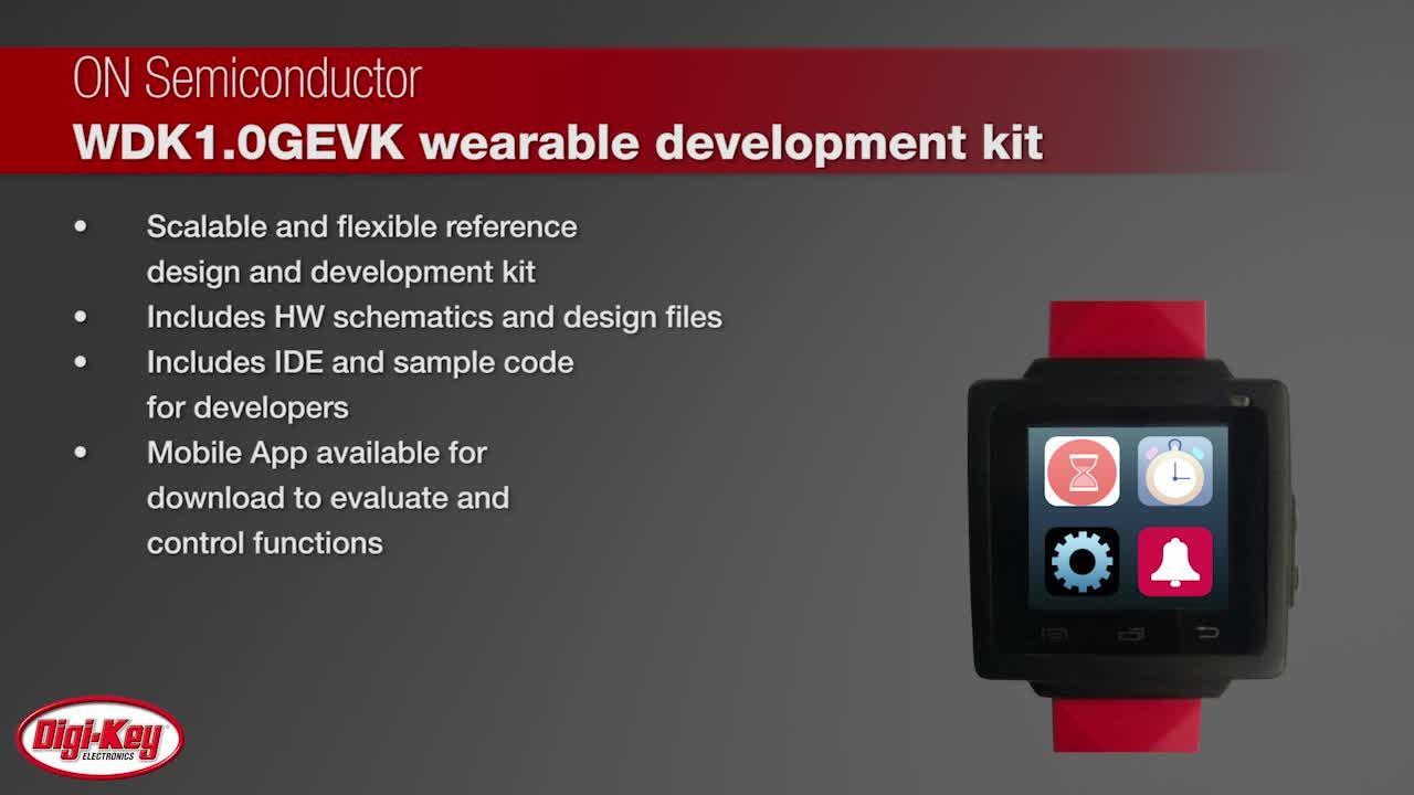
Few established enterprises and even fewer startups have the skills and experience needed to rapidly turn these requirements into competitive, differentiated products. The ON Semiconductor Wearable Development Kit (WDK1.0) is intended to address this need, showing developers how the required set of low-power ICs can be combined to create a complete, power-efficient wearable application solution (Figure 1).
")
Figure 1: The ON Semiconductor Wearable Development Kit provides a complete wearable multi-sensor touchscreen design as well as an associated docking station. (Image source: ON Semiconductor)
Similar to a smartwatch in configuration, the wearable device itself offers a touchscreen display designed to display output from the device's integrated motion and temperature sensors. For software development, ON Semi provides firmware and sample application code within an Eclipse-based integrated development environment (IDE). In addition, ON Semi also provides an associated mobile app (Android and iOS) designed to display activity-related information gathered from the wearable device.
At the heart of the hardware design for this wearable device is the Nordic Semiconductor nRF52832 MCU, which meets multiple responsibilities for system function. At the device level, the nRF52832 serves as a host for the sensors and peripherals. At the software services level, the nRF52832 also executes the middleware comprised of the communications protocol software stack, power management, and wireless charging library. Finally, the nRF52832 runs the software that provides the user with the desired application-level functionality.
The nRF52832 is well suited to its multiple roles in the design. The MCU integrates a high-performance 32-bit ARM® Cortex®-M4F processor core and a multiprotocol 2.4 GHz radio along with 64 kB RAM, 512 kB flash, and multiple analog and digital peripherals. As a result, the device can be configured to support a variety of connected applications with communications protocols including Bluetooth low energy (BLE). The device even includes an NFC-A tag that can be used for secure out-of-band pairing with other Bluetooth-enabled products.
The 32-bit M4F core provides hardware support for floating-point and digital-signal processing instructions. The combination of these efficient instructions and the high code density of the 32-bit core enables the MCU to deliver high-performance software execution out of a small code footprint. For example, even with the supported radio protocol stacks, as much as 400 kB flash is generally available for application software.
Sensor capabilities
For on-chip peripherals, the device features a 20-channel programmable peripheral interconnect (PPI) subsystem that supports peripheral operations without CPU intervention. Developers set dedicated PPI registers to connect a task to a hardware event through a PPI channel. For example, engineers can use this mechanism to cause an event occurring in a peripheral to trigger a task in a different peripheral. Besides reducing latency of peripheral-to-peripheral interaction, the PPI subsystem helps reduce overall power consumption by allowing peripheral operations such as data collection while the CPU remains in low-power mode.
For most wearable products, however, application requirements typically drive the need for complex sensors beyond those built into even the most advanced MCUs. The WDK1.0 addresses this need by demonstrating the integration of ON Semi's MEMS-based FIS1100 inertial measurement unit (IMU) IC and its associated sensor-fusion software. The FIS1100 IMU device combines motion sensors including a 3‐axis gyroscope and 3‐axis accelerometer, 16-bit analog-to-digital converters (ADCs), and a motion digital signal processor called the AttitudeEngine. This specialized engine is designed to automatically sample the sensor at a high rate and convert the raw sensor data into motion parameters required for higher level spatial orientation applications.
To generate application-level orientation information, ON Semi pairs the FIS1100 IC with its own XKF3 software library. The XKF3 library provides background auto-calibration services and includes nine-axis sensor-fusion algorithms that use the FIS1100 output to generate quaternion-format orientation information.
As the WDK1.0 design demonstrates, the hardware connection between the nRF52832 host and sensors is easily made through any of the MCU's various supported serial interfaces including SPI, I2C, or UART. The FIS1100 for example supports both SPI and I2C so the interface design is particularly simple. The FIS1100 connects to the host processor through its supported SPI or I2C serial interface to deliver quaternion motion information used by the XKF3 library (Figure 2).

Figure 2: Integrated sensors such as the ON Semiconductor FIS1100 inertial measurement unit completely encapsulate complex functionality such as motion encoding. (Image source: ON Semiconductor)
The software execution is equally simple. The nRF52832 host can poll the IMU to acquire this data simply by writing the value 0x0C into the IMU's dedicated CTRL9 register through the SPI or I2C bus. In the FIS1100, the CTRL9 register provides a mechanism for the host to initiate execution of predefined functions in FIS1100 firmware. Besides the value 0x0C for initiating host-directed data polling, the CTRL9 protocol defines values to set sensor correction values, manage the internal FIFO, and perform other configuration functions.
Along with host-directed data polling, the FIS1100 provides another mechanism designed to help reduce overall power requirements. Here, developers can program the device output data rate (ODR) across a wide range. For example, engineers can set the ODR for the device's quaternion motion data as low as 8 Hz.
Power management
The devices included in the WDK1.0 offer a number of power conservation mechanisms. For example, along with power savings through low ODR, the FIS1100 provides a "wake on motion" capability that allows the IMU to remain in low-power mode between physical activities. In any MCU-based design, however, the MCU is typically the most power-hungry device, so advanced MCUs such as the nRF52832 feature a number of power-saving features. As noted above, the nRF52832's PPI subsystem enables engineers to keep the MCU in low-power mode during peripheral operations. In fact, the nRF52832 can automatically shut down its own individual system blocks and peripherals when not needed for a particular task. At the same time, the MCU can quickly resume operation, requiring only a few microseconds to transition from low-power mode to an active execution state.
For a battery-powered design, however, power management requirements extend beyond power conservation itself. These designs also require an efficient mechanism for battery charging and charge management. Further, a wearable design must provide a charging process that is as simple as possible for the wearable's user. In this case, the WDK1.0 addresses this need by demonstrating both wired and wireless charging mechanisms.
For wired charging, the wearable device connects to its dedicated docking station through a pogo pin connector. For wireless charging, the wearable device itself is designed to support an industry-standard wireless charging protocol from the AirFuel Alliance. Although the docking station does not support wireless charging, ON Semiconductor notes that the wearable device can be wirelessly charged with any AirFuel-compliant charging station.
Although a deep description of the AirFuel wireless charging approach is beyond the scope of this article, its basic mechanisms use familiar technologies. In brief, the AirFuel protocol uses magnetic inductance among its supported technologies to transfer power from a charging station (Power Transmitting Unit or PTU) to a chargeable device (Power Receiving Unit or PRU). A unique aspect of the AirFuel protocol is its use of Bluetooth communications for charge-management monitoring and control.
Fortunately, wearable device developers do not need to become wireless charging experts to exploit this capability. In fact, the nRF52832 MCU's integrated Bluetooth radio virtually eliminates any hardware barriers to the implementation of this approach. With its nRF5 SDK for AirFuel, Nordic Semiconductor provides drivers and complete sample applications of the AirFuel protocol. As a result, software control of an AirFuel-compliant wireless charging session is as simple as a few function calls to initialize the BLE stack, the PRU (the wearable device), and start the PRU monitoring process (Listing 1). The underlying library provides the necessary software services and drivers for managing the AirFuel-compliant wireless charging process.
Copy
int main()
 {
    APP_TIMER_INIT(APP_TIMER_PRESCALER, APP_TIMER_OP_QUEUE_SIZE, false);

     m_ble_stack_init();

     pru_init(NULL);

 #ifdef DFU_SUPPORT
     // Set up button used for entering DFU mode
     common_hal_buttons_init(PRU_BUTTON_PRESS_LENGTH_DFU_MS, APP_TIMER_PRESCALER);
 #endif

     pru_start();

     while(1)
     {
         #ifdef DEBUG_OUT_ENABLE
         debug();
         #endif
     }
 }
Listing 1: As shown in this application-code snippet from the Nordic Semiconductor nRF5 SDK for AirFuel, developers invoke AirFuel-compliant services running on the Nordic nRF52832 MCU simply by initializing the BLE stack, the wearable (PRU), and optional device firmware update (DFU) support before starting the PRU process itself (pru_start()). (Code source: Nordic Semiconductor)
Power scheme
The combination of a complex MCU and different ICs with their own supply requirements can represent a significant challenge to efficient power management. Add in the need to manage a Li-ion battery with both wired and wireless charging options, and developers can quickly find themselves chasing a power budget even tighter than expected for a wearable design. In the WDK1.0, ON Semiconductor solves this problem with a simple power scheme designed ultimately to deliver regulated power to a system power management IC (PMIC) (Figure 3).

Figure 3: The ON Semiconductor wearable development kit uses a power scheme that ultimately delivers regulated power from a Li-ion battery to a system power management IC (PMIC) that provides the multiple supply rails required in this complex design. (Image source: ON Semiconductor)
System PMICs such as the ON Semi NCP6915 used in the WDK1.0 are low-power devices that integrate multiple converters and low dropout regulators to support multiple rails. In the WDK1.0, a buck-boost regulator drives the system PMIC with regulated output from the wearable's Li-ion battery to complete the supply-output side of the power scheme.
The power-input side addresses the need to deliver power reliably to the lithium-ion rechargeable battery from either wired or wireless sources. For Li-ion battery management, the WDK1.0 uses an ON Semi NCP1855 battery charger IC paired with an ON Semi LC709203 battery fuel gauge for charge management (Figure 1, bottom right). Finally, to supply power to the battery charger, the power scheme uses a basic power switch to select the wired or wireless charging source.
Conclusion
For consumers, wearable products provide instant information about the user and their immediate environment. For developers, however, wearable applications present a series of particular challenges. The ON Semiconductor wearable design kit offers a complete solution designed to help remove the many obstacles encountered during product development. By building on this kit, developers can rapidly create sophisticated wearable products that differentiate themselves with features such as advanced wireless charging.
聲明:各作者及/或論壇參與者於本網站所發表之意見、理念和觀點,概不反映 DigiKey 的意見、理念和觀點,亦非 DigiKey 的正式原則。