Power Modules and Devices to Support Intermediate Bus Architecture Designs
資料提供者:Electronic Products
2012-05-01
Almost three decades ago, the “brick” DC/DC converter power module was developed, which eventually led to the distributed power architecture (DPA) becoming the de facto standard for point of load (POL) designs. Soon, cost and board footprint became an issue and designers searched for alternative solutions for their power management architectures.
This article will discuss one of the more recent and popular power architectures emerging as a solution to designers’ problems, the intermediate bus architecture (IBA).
To deal with the size and cost constraints of DPA, second-generation systems moved to a fixed-voltage intermediate bus architecture or IBA (Figure 1).
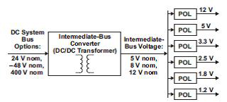
An IBA uses a single, isolated-brick, regulated power module and numerous non-isolated, point-of- load (POL) DC/DC converters. The POLs can be either power modules, such as the Texas Instruments (TI) PTH05010 series and the Emerson Network Power PTH12010 series (both part of the second source Point of Load Alliance), micro-modules like Linear Technology’s LTM4604, or discrete buck converters such as the Maxim MAX1920 series .
In many applications, the IBA-based power system includes a front-end AC/ DC power supply with a typical output of 24 V (such as CUI’s VOF-6-24) or 48 V (such as CUI’s VSK-S15-48U). In some data communications and medical equipment, the input DC voltage can be from a 400 V power-factor-corrector block. This voltage is supplied to an intermediate bus converter (IBC) that provides isolation and conversion to the lower-level intermediate bus voltage, typically ranging from 5 to 14 V. This intermediate bus voltage is supplied to nonisolated POL regulators that provide high-quality voltages for a variety of digital and analog electronic blocks.
The voltage choice is up to the system designer. This design results in less board space, lower cost, and easier sequencing of the voltages. The only drawback of this architecture is reduced efficiency, due to the double conversion required for each voltage.
Today, most telecom systems use a fixed-voltage IBA. For designers that need a higher-efficiency and smaller-footprint solution, they are directed towards the unregulated intermediate bus architecture, which creates an output voltage as a ratio of the input voltage.
Better efficiency is always sought by designers. The main area of focus for improving efficiency is the front-end isolated converter, since all of the power goes through it. The sure way to increase isolated-converter efficiency is to run the converter at a fixed duty cycle and not regulate the output.
Unregulated voltage became possible when wide-input (4.5 to 14 V) pulse-width modulators (PWMs) and power modules were introduced. This architecture is limited by the bus converters’ typical maximum input range of 36 to 55 V, set as such to keep the input voltage to the POLs below 12 V. The 12 V maximum is necessary because, for POLs to generate output voltages of 1 V or less, the input voltage should not usually exceed 10 to 12 times the output. However, a designer might consider a move to this limited input range for the significant cost savings, size reduction, and efficiency improvements obtained with this architecture.
These benefits are possible because they are unregulated (less complexity and cost) and can operate at a constant 50 percent duty cycle (higher efficiency). The IBC output voltage is constrained to a fixed value as determined by the turns ratio of the IBC transformer. The IBC therefore can be considered a “DC transformer.”
A 4:1 turns ratio with a nominal 48 V input provides the nominal 12 V output from the IBC. Other commonly used turns ratios are 3:1 and 5:1, resulting in nominal bus voltages of 15 and 9 V respectively. The individual POL converters accomplish the regulation of each of the output voltages (Figure 2).
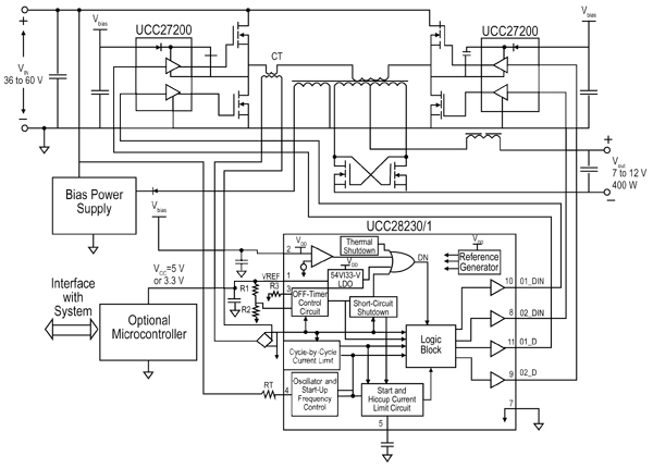
Systems with a high total output power tend to favor the unregulated bus architecture, especially if high current or power levels are present on two or more output voltages. The regulated bus approach is often the best choice for lower power systems with most of the output power concentrated on one output voltage.
Some telecom OEMs insist on maintaining the traditional, wider input voltage specification of 36 to 75 V with input transients of up to 100 V. For these requirements, the power industry has responded with the quasi-regulated IBA. The main difference between this and the unregulated IBA is that if the input voltage exceeds 55 to 60 V, the quasi-regulated IBA regulates the output voltage to around 10 V. The drawback of this approach is that the isolated power module must increase in size to accommodate the regulation circuitry, and its efficiency is reduced when the input voltage exceeds 55 V.
In today’s challenging business environment, solutions abound using distributed voltage bus standards such as the 12 V Intermediate Bus Architecture (IBA). The deployment of low-cost unregulated (open-loop) bricks to convert from the 48 V bus to a standard 12 V intermediate bus has allowed low cost Point-of-load (POL) modules to be used. These small form-factor POL modules, available in single in-line package (SIP) and surface-mount device (SMD) packages, provide a cost-effective means of providing system loads with multiple low-voltage supplies.
References:
- Texas Instruments, “Power-management solutions for telecom systems improve performance, cost, and size,” by Brian C. Narveson and Adrian Harris Application note #SLYT278, 2007
- Texas Instruments, “Improving System Efficiency with a New Intermediate-Bus Architecture,” by Rais Miftakhutdinov
- Vicor, “Innovative Power Device to Support Intermediate Bus Architecture Designs,” by Jeffrey A. Ham, Douglas Ping
聲明:各作者及/或論壇參與者於本網站所發表之意見、理念和觀點,概不反映 DigiKey 的意見、理念和觀點,亦非 DigiKey 的正式原則。


