Applying Chip and Patch Antennas to Solve Diversity and Multiband RF Issues
2017-05-25
Designers of handheld and portable wireless products such as smartphones and wearables rely on tiny chip, patch and trace antennas that can be placed within the device. While these miniature devices solve the problem of bringing multiband antenna arrays to small form factor systems, they also introduce issues related to reduced radiation efficiency, impedance matching, and interaction with nearby objects and bodies.
To address these problems, designers are being armed with new design and circuit techniques to make these antennas more than just a standalone component. Instead, they are becoming part of a dynamic antenna subsystem that mitigates many of these design challenges. This shift in design requires extensive simulation and analysis, which is being addressed by constantly improving field solver software.
Chip, patch antennas offer tradeoffs
There are many reasons to move from traditional, external whip or stub antennas to chip and patch antennas, starting with aesthetics and the fragility of external antennas. From a performance point of view, devices such as smartphones often need multiple antennas for a given band to provide antenna diversity for improved performance. In addition, multiband devices – especially those for devices compatible with the emerging 5G standard– will need separate, independent antennas for each band they must support. While the reasons are many, chip and patch antennas have their own tradeoffs.
Chip antennas use a multilayer ceramic structure to form a component that is resonant at a target frequency (Figure 1). They are small and easily placed on a PC board, just like any other surface-mount component.
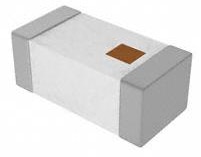
Figure 1: Without the extremely small, low cost and easy to apply ceramic-based chip antenna, many portable wireless devices would be impractical. Shown is the Johanson Technology 2450AT18B100E, which is centered on the widely used 2.4 to 2.5 gigahertz band. (Image source: Johanson Technology)
Two examples illustrate their features. The Johanson Technology 2450AT18B100E is a 1.6 x 3.2 millimeter chip antenna for the 2.4 to 2.5 gigahertz (GHz) band, with nearly omnidirectional radiation pattern regardless of orientation, despite its small size (Figure 2). Antennas such as this have been used extensively and successfully in portable and handheld wireless devices. While the chip antenna itself is simple, designers must match the associated drive circuitry to its standard 50 Ω impedance. This may become a challenge when multiple chip antennas are used in a diversity architecture.
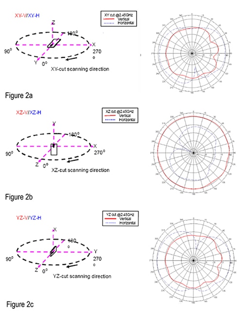
Figure 2: Johanson characterizes the chip antenna’s radiation pattern for all three axes, shown top to bottom: a) XY, b) XZ, and c) YZ; note that the pattern is fairly omnidirectional for all three. (Image source: Johanson Technology)
Another chip antenna is the Taiyo Yuden AF216M245001-T, constructed to emulate a monopole helical antenna, also for 2.4 to 2.5 GHz operation. Measuring 2.5 x 1.6 mm, the antenna also has fairly omnidirectional characteristics, and maintains a VSWR of under 2:1 from 2.45 GHz to 2.7 GHz (Figure 3).
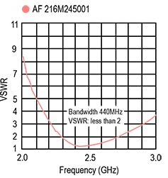
Figure 3: Taiyo Yuden’s AF216M245001-T chip antenna maintains a 2:1 VSWR across its primary bandwidth of operation, 2.45 GHz to 2.7 GHz. (Image source: Taiyo Yuden)
As chip antennas are inexpensive, small, and easy to work with, it would seem they are the optimum solution for many wireless needs. While this is often the case, the reality is that like all components, they present tradeoffs. In this case, it is their relatively low typical efficiency of 40% to 50%, along with their susceptibility to both fixed and changing ambient conditions which include pc board layout, nearby components, and the user.
An alternative to the chip antenna is the patch antenna (Figure 4). While larger than the chip design, it is fairly flat and therefore can often be positioned along the inside of the product enclosure, away from components and other sources of radiation pattern distortion.
Patch antennas, such as the W6112B0100 from Pulse Electronics, support 2 by 2 multiple input, multiple output (MIMO) LTE applications including smart meters, remote monitoring, and IoT designs. Though larger than the chip antenna – about 8.8 inches long × 0.8 inches high – this antenna boasts an efficiency of 55% to 75%, depending on the specific band it is supporting (Figure 5).
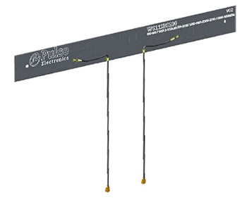
Figure 4: The patch antenna, such as the multiband W6112B0100 from Pulse Electronics, does not mount on a pc board, but is attached to the inside of the product enclosure, away from the board and circuitry. (Image source: Pulse Electronics)
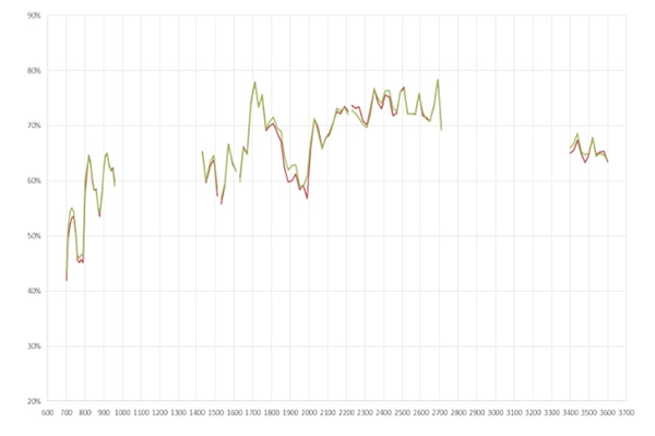
Figure 5: The W6112B0100 for 2 by 2 MIMO 4G/LTE is designed to operate and maintain efficiency across multiple bands of 698 MHz to 960 MHz, 1.428 GHz to 1.51 GHz, 1.559 GHz to 1.61 GHz, 1.695 GHz to 2.2 GHz, 2.3 GHz to 2.7 GHz, and 3.4 GHz to 3.6 GHz. (Image source: Pulse Electronics)
A third antenna option is the pc board trace approach, which uses one or more etched layers of the pc board to create the antenna. This solution has no direct BOM cost and is extremely flexible as it can be used to create custom or unique antennas which cannot be realized using discrete components. A single trace antenna can cover multiple bands, include filtering, and support multiple polarizations.
But there is no “free lunch” as the trace antenna usually requires a significant amount of pc board real estate, and its performance is greatly affected by the nearby layout, component placement, and component type. The gap between a theoretical trace antenna and its actual installation is fairly wide, and can be frustrating to overcome.
When a system has multiple antennas, there is also the issue of how to switch among them if the topology requires this function. Electromechanical switches are effective and have excellent electrical specifications, but are obviously not practical for small or portable devices, or those with a need to switch quickly. Instead, electronic switching must be used, usually based on PIN diodes (see, “How and Why to Use PIN Diodes for RF Switching”) or solid-state switches (see, "Semiconductor RF Switches: Small But High-Performing Circuit Components"). The latter are much easier to use and design into circuits than switches based on PIN diodes, although sometimes the attributes of the PIN diode are required.
For example, the Peregrine Semiconductor PE42422MLAA-Z is a basic SPDT RF switch with no moving parts that is suitable for operation from 5 MHz to 6 GHz. It can be designed into a circuit with few design challenges (Figure 6). This 50 Ω component, in a tiny 12-lead 2 x 2 mm QFN package, combines on-board CMOS control logic with a low-voltage, CMOS compatible control interface and requires no external components. It typically switches between channels in 2 microseconds.
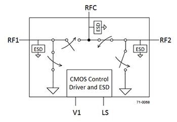
Figure 6: When there are multiple antennas, it is often required to switch the RF signal path among them. An all-electronic RF SPDT switch such as the Peregrine Semiconductor PE42422MLAA-Z provides a way to do this via simple installation and control, and with a 2 microsecond switching time over a range of 5 MHz to 6 GHz. (Image source: Peregrine Semiconductor)
Insertion loss ranges from 0.23 dB at 100 MHz to 0.9 dB at 6 GHz, while the third-order intercept point (IIP3) is 75 dBm (minimum) across the entire range. With a switch such as this, an RF signal is easily routed to/from a common port to either of two independent ports, with isolation of 68 dB at lower frequencies, to 17 dB at higher frequencies. The insertion loss is between 0.23 and 1.25 dB, again depending on frequency.
Advanced techniques address real-world problems
The performance of any antenna is affected by its surroundings including nearby components, shielding, and packaging. The effects of these elements can be modeled and then accommodated into the final design, although this often takes multiple interactions to balance the competing demands (see, “Understanding Antenna Specifications and Operation, Part 1” and “Understanding Antenna Specifications and Operation, Part 2“.
For compact portable and handheld devices, however, the problem is much more complex because the antenna surroundings constantly change. Users may hold the product at different orientations or close to different parts of their body (wrist, head, or torso), or place it near to other objects while in use. As a result, the antenna is in a less than optimum situation where the effective impedance and resonant frequency of the antenna will change and degrade performance.
When the antenna resonant frequency shifts, the impedance it presents to the rest of the radio front end shifts away from an initial value, causing an impedance mismatch. This mismatch has three effects. More energy is reflected from the antenna terminals rather than passing through the terminals, the output power from the power amplifier (PA) drops due to load pull, and the antenna’s radiation efficiency is reduced due to capacitive loading.
This antenna situation has been degrading the RF link budget for the past few decades, compromising performance of the product. This degradation has not been noticed by users due to improvements in network wide and system level performance. More cell sites, the use of cell site antenna beamforming, and improved error correction techniques have largely compensated for it. Such compensation may no longer be adequate due to increased system level and user demands, especially for the emerging 5G standard.
There are three loss modes associated with this situation: absorption loss, impedance mismatch loss, and antenna radiation efficiency loss. Absorption loss can be as high as 8 to 10 dB and there is little that can be done about it (at present). Impedance mismatch losses are about 1 to 2 dB, and antenna radiation efficiency loss is about 2 to 3 dB. Impedance mismatch and radiation efficiency loss can be recovered in two ways: by changing the antenna’s matching circuitry and by changing the resonance of the antenna.
Wireless device vendors have addressed the problem in the latest generations of their devices. Dynamic tuning can compensate for the head and hand effects causing shifts of the antenna’s resonant frequency. This is done via a closed-loop tuning cycle to reduce the mismatch between the antenna and the PA to optimize power transfer (Figure 7).
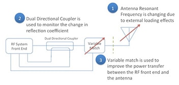
Figure 7: Closed-loop tuning is used to dynamically modify the impedance matching network for optimum performance and recued losses. (Image source: Antennasonline.com)
In closed-loop tuning, the inevitable changes in the reflection coefficient are detected in real time. This is done by monitoring both the magnitude and phase of the forward and reflected power at the terminals of the antenna via a directional coupler (see, "Tiny Directional Couplers Meet Demands of Compact RF Applications"). The system then synthesizes a complex conjugate that is used to adjust the match network located at the antenna feed point to enhance RF power transfer between the front end and the antenna. This reduces losses by as much as 1 to 3 dB.
While useful, this closed-loop tuning technique has several drawbacks. Measuring the magnitude and phase of the reflection coefficient, and then determining the conjugate match requires significant computational cycles and time, or use of a lookup table. The lookup table is faster but less accurate. In order to implement a complex match, a complex matching circuit is required. The performance improvement achieved using this approach is typically between 1 and 3 dB.
An alternative to closed-loop tuning is aperture tuning, which is often used in conjunction with impedance matching. Here, instead of adjusting the matching network to accommodate changes in antenna impedance, the antenna size (tuning state) is changed electrically to restore its resonance to the point of maximum power transfer (Figure 8). This requires a large number of closely spaced tuning states.
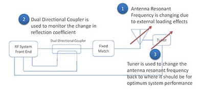
Figure 8. An aperture-tuned antenna dynamically adjusts the resonant length of the antenna to minimize losses. (Image source: Antennasonline.com)
Here, the reflection coefficient is measured at the antenna feed terminals, as was done for closed-loop tuning. Next, one of several approaches is used with this measurement to determine the best new tuning state. Three of these approaches are scalar techniques and require monitoring only the magnitude of the reflected power at the antenna terminals using a simple directional coupler, then applying different calculation approaches (known as least squares fit, threshold tuning, or trough detection).
The fourth technique is vector-based and uses both the magnitude and phase of the reflection coefficient to determine S-parameter matrix solution for the antenna structure, and then the tuner setting that is required to restore the antenna’s resonant frequency. A reduction of 2 to 4 dB in loss is typical. When combined with impedance matching, the overall improvement ranges from 3 to 7 dB.
Modeling and simulation critical to design success
For an external antenna such as a standard whip design, there is little or no need to model performance early in the design cycle. However, for chip, pc-board trace, and even patch antennas located a short distance from the low-noise amplifier or PA, simulation of the antenna and its implementation are critical. It is not possible to build, test, modify, repeat, and iterate to find a suitable configuration. Not only must the antenna be modeled, but the entire surrounding environment of the pc board, components, case, and even user hands or head position must be modeled and analyzed.
Fortunately, there are many sophisticated electromagnetic field solver application packages that address the simulation issues. These are supported by powerful PCs or cloud-based computational platforms that can run the extensive calculations these field solvers need for their analysis. These field solvers can also analyze the effect of design tolerance through minimum/maximum trials or Monte Carlo runs across multiple variables. They can show where even a fraction of a millimeter change has significant effect at GHz frequencies, implement “what-if” analysis to investigate the effects of possible design changes, and also highlight design weaknesses or unexpected characteristics.
Conclusion
Despite its functional simplicity, the antenna is a complicated electromagnetic transducer that converts the electrical power in circuitry into an electromagnetic field, and vice versa. Traditional single element antennas, such as the dipole and whip, are now augmented with one or more antennas that use multilayer ceramics, flat-patch construction, and even the product’s own pc board.
Incorporating these antennas into compact, often portable products requires careful analysis of the complete system and package to verify that the antenna’s idealized performance is not excessively compromised, and will meet the design objectives. This is made possible with field solver software that supports detailed modeling and associated calculations of the electromagnetic fields and antenna performance in the actual installation.
聲明:各作者及/或論壇參與者於本網站所發表之意見、理念和觀點,概不反映 DigiKey 的意見、理念和觀點,亦非 DigiKey 的正式原則。


