How to Wield the Power of the Bode Plot to Ensure Circuit Stability
In the 1930s, Hendrik Wade Bode created an intuitive gain/phase approach, with a circuit’s stability as the sole objective. This became what is now called the Bode plot, an intuitive graphical display of a circuit or amplifier’s gain, phase, and feedback system, over frequency.
Given its usefulness and importance, let’s take some time to apply a Bode stability analysis technique to look at an open-loop amplifier and circuit feedback factor magnitude, in decibels (dB) and phase response (in degrees). This blog will look at these concepts and suggest how to avoid designing a “warbling” circuit when your primary objective is frequency stability.
To practice this technique, you can download a printable version of a Bode plot graph from the resources in the online DigiKey Innovation Handbook.
Single-pole Bode plot
The configuration of the single-pole circuit allows DC VIN signals to go directly to VOUT, while at higher input frequencies, VOUT equals zero decibels (dB). The Bode plot construction is simple. The y-axis units are logarithmic frequency, and the linear x-axis is either gain in decibels or phase in degrees. There have been a significant number of formulas that you can apply when designing a Bode plot, but let’s cut to the quick solution approach.
The simplicity of the Bode plot is that the drawing of the graphs only requires a straight edge tool and the knowledge of a few rules (Figure 1).
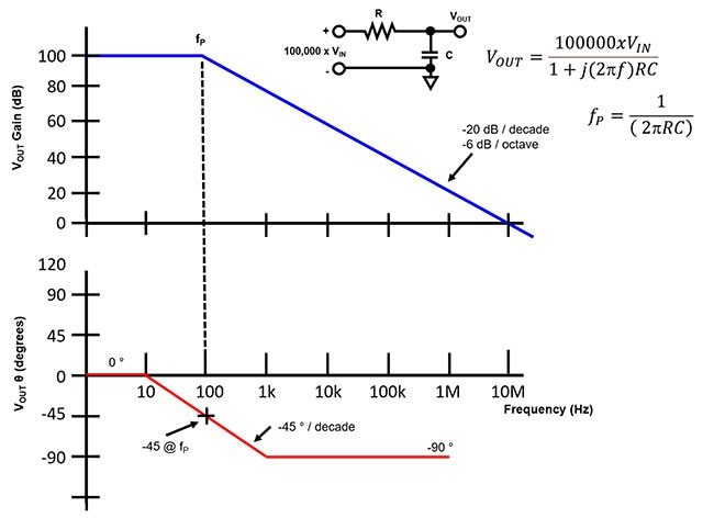 Figure 1: A single-pole Bode plot illustrating magnitude and phase shift uses straight lines to illustrate the circuit’s frequency and phase response. (Image source: Bonnie Baker)
The two plots in Figure 1 represent the frequency versus gain and phase for a single-pole resistor/capacitor pair. The top and bottom plot’s x-axis frequency ranges are from 1 Hertz (Hz) to 10 megahertz (MHz). The top plot y-axis range is from 0 decibels (dB) to 100 dB, with the 1 Hz signal value equal to 100 dB. This value is consistent with a gain factor of 100,000 x VIN. The blue curve is the gain response with a single-pole at fP or 100 Hz, where R equals 159 kilohms (kΩ), and C equals 10 nanofarads (nF).
As frequency increases past the pole frequency (fP), the blue curve falls at a -20 dB/decade or -6 dB/octave rate. This rate of attenuation is the first Bode plot rule-of-thumb to remember: Every pole in the circuit falls at a -20 dB/decade rate, starting at the pole frequency. Thus, if two poles attenuate VOUT in the same frequency range, the attenuation rate is -40 dB/decade.
The Figure 1 bottom plot represents the phase of this single-pole circuit. At 1 Hz, the phase of the R/C network is 0 degrees (°). At a decade before fP, or in this case 10 Hz, the single-pole phase starts falling at a -45°/decade towards its -90° target.
Several rules apply to the pole’s phase response. The second Bode plot rule-of-thumb for the pole circuit is that the phase equals -45° at fP. The third and fourth Bode plot rules describe the phase point of attenuation and completion. The single-pole phase starts to fall one decade before the pole frequency (fP), and finally settles one decade after fP at -90°.
Single-zero Bode plot
The single-zero Bode plot reflects the opposite rules of the single-pole Bode plot. The positions switch with the same values for R and C to prevent DC VIN voltages, while allowing the higher frequency to pass through the capacitor (Figure 2).
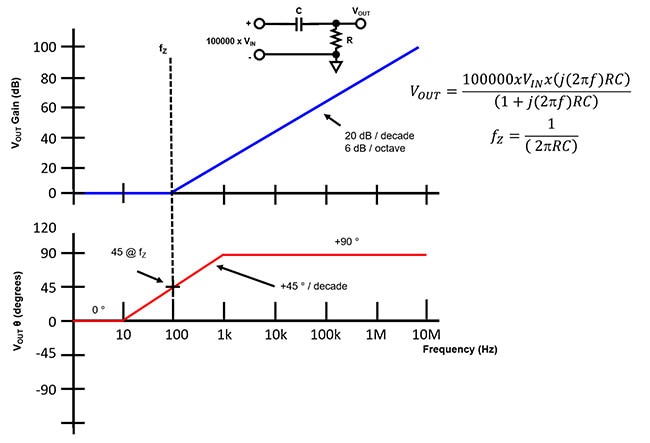 Figure 2: Single-zero Bode plot illustrating magnitude and phase shift. (Image source: Bonnie Baker)
As frequency increases beyond fZ, the blue curve rises at a +20 dB/decade. The Figure 2 bottom plot represents the phase of this single-zero circuit. At a decade before fZ, the single-zero phase starts rising at a +45°/decade rate towards its +90° target. The zero circuit phase equals +45° at fZ.
To summarize the values in Figure 1, the pole location is fP, and the gain magnitude after fP has a -20 dB/decade slope. The phase has a -45°/decade slope through fP, and the phase starts its attenuation at 0.1x fP and settles to -90° at 10 x fP. To summarize the values in Figure 2, the zero location is fZ, and the gain magnitude after fZ has a +20 dB/decade slope. The phase has a +45°/decade slope through fZ, and the phase starts its attenuation at 0.1 x fZ and settles to +90° at 10 x fZ.
Amplifier open-loop Bode plot
The frequency operation of the standard operational amplifier (op amp) product can have multiple poles and zeros in the transfer function from sub-hertz to the zero-dB cut-off frequency. There is no magic in the amplifier Bode plot; just follow the rules (Figure 3).
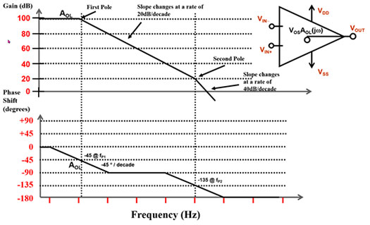 Figure 3: Possible Bode plot of an op amp illustrating magnitude and phase shift. (Image source: Bonnie Baker)
Figure 3 illustrates an op amp example with two poles (f1 and f2) in the transfer function. With the two poles, the gain falls -20 dB/decade each time, and the phase falls to a total of -180 degrees.
At this point, we have a good start on how to construct Bode plots, but let’s move forward towards the real world, where there is a feedback system in the mix.
Closed-loop amplifier system stability
You will always find a feedback network hanging around if you take some time to look at op amp circuits. The classical op amp feedback network has a gain forward element (AOL(jω)) and the feedback element (β(jω)).
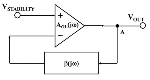 Figure 4: Classical op amp feedback network with a feed-forward element (AOL(jω)) and feedback element (β(jω)). (Image source: Bonnie Baker)
In Figure 4, the open-loop gain of the op amp (AOL) is comparatively large, and the feedback factor is relatively small. This configuration sends the output back to the inverting terminal creating a negative feedback condition, where this feedback brings the output under control. We will use the inverse of β or 1/β to determine an op amp circuit’s stability.
The easiest way to calculate 1/β is to place a source, called VSTABILITY, on the op amp’s non-inverting input. This calculation strategy will provide an excellent path to determine the circuit’s stability (Figure 5).
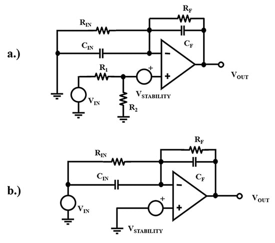 Figure 5: A non-inverting op amp circuit a.) and inverting op amp circuit b.) both have a fictitious VSTABILITY voltage source at their non-inverting input to enable accurate calculation of the circuit’s 1/β factor, or noise gain. (Image source: Bonnie Baker)
If you examine the circuits in Figure 5, you will notice that the feedback circuits from the non-inverting terminal to the output are the same. The location of the VSTABILITY voltage source enables an accurate calculation of the circuit’s 1/β factor, or noise gain.
The 1/β stability analysis uses VSTABILTIY. If you assume the op amp open-loop gain is infinite, the transfer function of both circuits equals:
 Equation 1
 Equation 2
 Equation 3
When the Equation 3 frequency components, jω, is equal zero:
 Equation 4
As jω approaches infinity in Equation 3:
 Equation 5
The frequencies for 1/β’s zero (fZ) and pole (fP) are:
 Equation 6
 Equation 7
The Bode plots of the 1/β stability-analysis curves complying with the rules set above are shown in Figure 6.
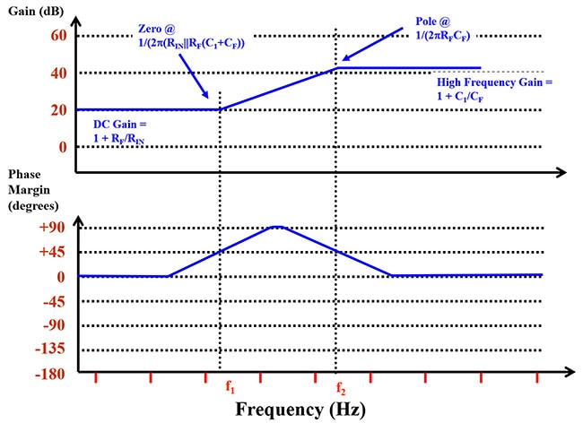 Figure 6: The 1/β frequency response for Figure 5 a.) and b.) are identical. The zero occurs at a lower frequency, and the pole occurs at a higher frequency. (Image source: Bonnie Baker)
Figure 6 describes the frequency and phase response of the op amp circuit’s 1/β, or noise gain. This figure summarizes equations 4 through 7 in graphical form. Equations 4 and 5 define the DC gain and ¥ gain, inclusively. Equations 6 and 7 identify the circuit’s zero and pole, inclusively. The information in Figures 3 and 6 provides the first step in establishing an op amp circuit’s stability by defining the system’s transfer function and location of the poles and zeros. The final step is to superimpose Figures 3 and 6 into one graph.
System stability determination
The intersection or rate of closure of the open-loop and the closed-loop gain defines the phase shift of the circuit. Generally, a closure rate less than or equal to 30 dB indicates a stable circuit. A rate of closure greater than 30 dB is moving towards an unstable circuit condition (Figure 7).
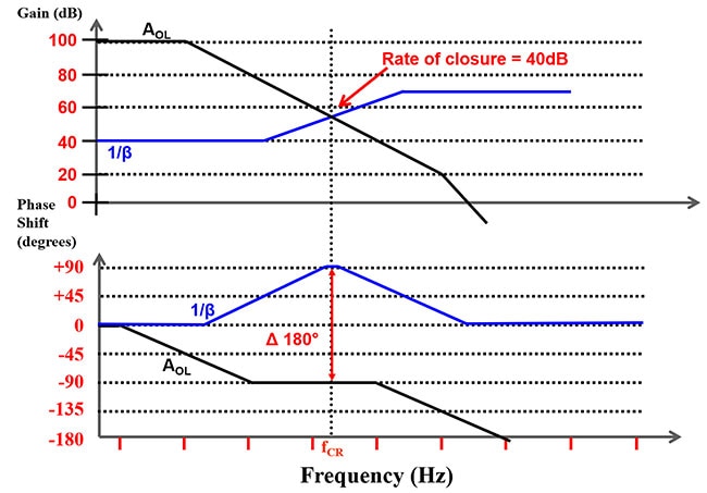 Figure 7: Superimposed op amp’s AOL gain and phase response with the 1/β gain and phase response. (Image source: Bonnie Baker)
In Figure 7, the rate of closure between the AOL and 1/β gain curves is equal to 40 dB. A 40 dB rate of closure indicates a phase shift greater than 135°, which shows an unstable circuit. With this configuration, the rate of closure of 180° produces a circuit that oscillates.
There are many solutions to the above problem. The resistive or capacitive values can be varied by moving the pole and zero frequencies. Another alternative is to select a different op amp (Figure 8).
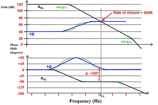 Figure 8: Using an op amp with a bandwidth that is higher than the op amp in Figure 7 without changing the zero and pole frequencies. (Image source: Bonnie Baker)
In Figure 8, the op amp bandwidth is approximately two decades higher without a change to the 1/β network. The green dashed lines reflect actual calculations and provide a more realistic Bode plot. The increase in amplifier bandwidth changes the rate of closure from 40 dB to 20 dB. The resulting phase shift is now ~105°, indicating a stable circuit.
The green dotted lines in Figure 8 go beyond the ruler and pencil creation of the bode plot by including the real-world response.
Measuring circuit gain and phase
Measuring an amplifier circuit’s gain and phase requires a function generator that provides the input signal, along with a network analyzer (Figure 9). Represented is the Tabor Electronics LS3081B 3 GHz RF analog sweep function generator.
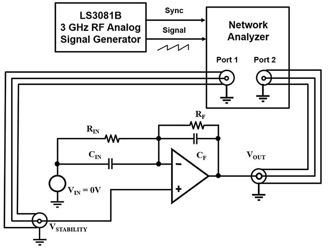 Figure 9: Gain and phase measurement configuration for Figure 5 b.)’s inverting amplifier circuit. (Image source: Bonnie Baker)
In Figure 9, the application of the function generator’s input signal occurs at Port 1 to VSTABILITY node. The signal propagates through the amplifier circuit to the circuit’s output (VOUT), where the network analyzer captures the signal at Port 2 and compares it to the function generator’s Port 1 signal.
Conclusion
When it comes to designing stable op amp circuits, the Bode plot is an extremely useful tool to add to your kit. The power behind the Bode plot becomes apparent when you start to look at multi-pole and multi-zero circuits, where the rate of closure between the amplifier open-loop gain and the feedback network quickly defines the stability of your circuit.
While this blog can help master the use of the Bode plot by showing the simple use of a straight edge on graph paper to estimate the gain versus phase of a first-order pole and zero circuit, the best way to learn is to practice. Again, you can start by downloading a printable version of a Bode plot graph from the resources in the online DigiKey Innovation Handbook.

Have questions or comments? Continue the conversation on TechForum, DigiKey's online community and technical resource.
Visit TechForum


