Understand and Minimize the Impact of Jitter on High-Speed Links
Contributed By DigiKey's North American Editors
2023-12-21
Clock oscillators provide the timing heartbeat of modern circuits by pacing system components. As system speeds increase to the hundreds of megahertz (MHz) and higher, these clocks must be faster and provide very low jitter, typically under 100 femtoseconds (fs), to maintain system performance. They must also maintain their low jitter specifications over time, despite variations in temperature and voltage.
Some jitter is induced by signal-path noise and distortion, and it can be somewhat reduced using reclocking and retiming techniques. However, jitter is also generated by the clock source, which is usually an oscillator. This is due to various physical phenomena, including thermal noise, process imperfections, power supply noise, other external noise getting into the clock oscillator, material stresses, and many other subtle factors. Regardless of the source, it is up to the designer to do everything possible to minimize inherent clock jitter, as the deficiencies are not reversible.
This article discusses jitter issues from various perspectives. It then introduces different clock oscillators from Abracon LLC and shows how jitter can be minimized by matching the clock oscillator performance to the application.
Jitter basics
Clock jitter is the deviation of a clock edge from its ideal position in time. This jitter affects the timing precision and accuracy of the transmission of data signals that the clock signal is pacing, leading to degradation of the signal-to-noise ratio (SNR) at the receiver decoding/demodulation circuitry or other system ICs. This results in a higher bit error rate (BER), increased retransmissions, and reduced effective data throughput.
Given its criticality, clock jitter is widely analyzed in systems that pass a signal from a transmitting source to a receiver over cables, connectors, or circuit boards. Depending on the application, it can be characterized in many ways, including cycle-to-cycle, period, and long-term jitter (Figure 1).
 Figure 1: The term “jitter” encompasses many timing variations, including cycle-to-cycle jitter, period jitter, and long-term jitter. (Image source: VLSI Universe)
- Cycle-to-cycle jitter signifies the change in clock period across two consecutive cycles and is unrelated to frequency variation over time.
- Period jitter is the deviation of any clock period with respect to its mean period. It is the difference between the ideal and actual clock periods, and can be specified as either root-mean-square (RMS) period jitter or peak-to-peak period jitter.
- Long-term jitter is the deviation of the clock edge from its ideal position over a longer period of time. It is somewhat analogous to drift.
Jitter can corrupt the timing used by other sub-functions, components, or systems used to achieve low BER data recovery, or pace components such as memory elements or processors in a synchronous system. It is seen in the eye diagram of Figure 2 as a widening of the crossover point in the bit timing.
 Figure 2: In an eye diagram, jitter is seen as a widening of the critical timing-crossover point in the data stream. (Image source: Kevin K. Gifford/Univ. of Colorado)
For serial data links, the circuitry at the receiving end must try to reestablish its own clock for optimal data-stream decoding. To do so, it must synchronize and lock onto the source clock, often using a phase lock loop (PLL). Jitter affects the system’s ability to do this precisely, compromising its ability to recover the data with a low BER.
Note that jitter can be measured in both the time and frequency domains; both are equally valid perspectives of the same phenomenon. Phase noise is a frequency-domain view of the noise spectrum around the oscillator signal, while jitter is a time-domain measure of the timing accuracy of the oscillator period.
Jitter measurements can be expressed in several ways. It is commonly cited using time units such as “jitter of 10 picoseconds” (ps). Root mean square (RMS) phase jitter is a time-domain parameter that is derived from the phase noise (frequency domain) measurement. Jitter is sometimes also referred to as phase jitter which can be confusing, but it is still the time-domain jitter parameter.
As link operating frequencies and their clocks speed up from a few tens of MHz into the hundreds of MHz and higher, the allowable jitter on the clock source decreases to around 100 fs or less. These frequencies apply to optical modules, cloud computing, networking, and high-speed Ethernet, all of which are functions and applications that require a carrier frequency between 100 and 212/215 MHz and data rates of up to 400 gigabits per second (Gbps).
Managing the crystal
The most common way to create a stable, consistent, accurate-frequency clock signal is to use a quartz crystal oscillator. An associated oscillator circuit supports the crystal. There are many such circuit families, each with various tradeoffs. Crystals have been used in this role since the 1930s for wireless radio communication in the medium-frequency (300 kilohertz (kHz) to 3 MHz) and high-frequency (3 to 30 MHz) RF bands.
One widely used approach to generate low-jitter clocks is to use one of the many variations on PLL-based architectures. For example, devices in Abracon’s AX5 and AX7 ClearClock™ families come in 5 × 3.2 millimeter (mm) and 5 × 7 mm packages, respectively, and use a sophisticated PLL technology for superior low-jitter performance (Figure 3).
 Figure 3: The Abracon AX5 and AX7 clock oscillators use one of the many PLL-based designs but with subtle enhancements to minimize jitter. (Image source: Abracon)
Along with operating frequency and oscillator design, jitter performance is affected by the physical size of the quartz crystal at the oscillator core. As the size of this crystal is reduced, it becomes more challenging to provide superior RMS jitter performance.
For clocking solutions in the 100 to 200 MHz band, and in smaller form factors than the PLL-based AX5 and AX7 devices, a new oscillator architecture is needed. These requirements for smaller sizes are typically associated with the latest-generation optical transceivers and modules. There are four established ways to design a clock oscillator in the range of 100 to 200 MHz:
- Use a quartz oscillator with an inverted mesa quartz blank as the resonator element
- Use a quartz oscillator with a third-overtone quartz blank as the resonator element
- Use an oscillator loop based on a sub-50 MHz, third-overtone/fundamental-mode quartz blank, or a sub-50 MHz, temperature-compensated crystal oscillator mated with an integer or fractional-mode PLL IC
- Use a sub-50 MHz microelectromechanical systems (MEMS) resonator-based oscillator loop mated with an integer or fractional-mode PLL IC
Option 1 does not offer the best RMS jitter performance, nor is it the most cost-effective solution. Option 3 gets complicated and has performance deficiencies, while the MEMS resonator approach of option 4 does not meet the primary performance criteria of 200 fs maximum RMS jitter. In contrast, option 2 uses an optimally designed third-overtone quartz blank with consideration given to the geometry of the electrodes and the optimization of the angle of cut. This combination is optimal in terms of cost, performance, and size.
Using this approach, Abracon developed “third overtone” ClearClock solutions (Figure 4). These devices use a quieter architecture to enable superior, ultra-low RMS jitter performance and extreme energy efficiency in miniature packages as small as 2.5 × 2.0 x 1.0 mm.
 Figure 4: The “third overtone” ClearClock solution from Abracon uses a quieter architecture to improve overall performance and energy efficiency. (Image source: Abracon)
In this scheme, careful design of the third-overtone crystal blank, along with the proper filtering and “trapping” of the desired carrier signal, ensures outstanding RMS jitter performance at the desired carrier frequencies.
This architecture does not use a typical PLL approach, so there is no up-conversion. Consequently, there is no need for standard PLL fractional or integer multiplication, and the final output frequency has a one-to-one correlation with the resonant frequency of the third-overtone quartz crystal. The absence of fractional or integer multiplication simplifies the design and enables minimum jitter in the smallest possible size.
Specifications and performance in reality
Clock oscillators are more than just a crystal and its analog circuit. They include buffering to ensure that the oscillator output load and its short and long-term variations do not affect the unit’s performance. They also support various differential digital logic output levels for circuit compatibility. This compatibility removes the need for an external logic-level translation IC. Such an IC would increase cost, footprint, and jitter.
As clock oscillators are used in so many diverse applications with different rail voltages, they must be offered in a variety of supply voltages such as +1.8 volts, +2.5 volts, or +3.3 volts, as well as custom values typically spanning from 2.25 to 3.63 volts. They must also be available with differing output-format options such as low-voltage positive/pseudo emitter-coupled logic (LVPECL) and low-voltage differential signaling (LVDS), as well as other formats.
A look at two families of crystal clock oscillators, the AK2A and the AK3A, demonstrates what can be accomplished through sophisticated understanding and integration of materials, design, architecture, and test. The two families are similar, with their standout differences being size and maximum frequency.
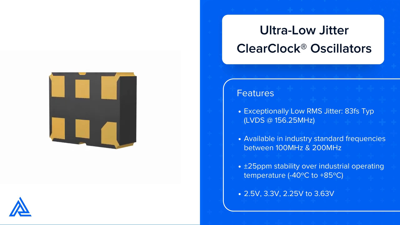
The AK2A family: This family of crystal oscillators is offered at nominal frequencies from 100 to 200 MHz and is available with operating voltages of 2.5 volts, 3.3 volts, and 2.25 to 3.63 volts with LVPECL, LVDS, and HCSL differential output logic.
All family members have similar performance, including low RMS jitter. For example, the AK2ADDF1-100.000T is a 100.00 MHz, 3.3 volt device with LVDS outputs and an RMS jitter of 160.2 fs (Figure 5). Its frequency stability is excellent at better than ±15 parts per million (ppm) over temperature, and it comes in a six-lead, surface mount device (SMD) package measuring 2.5 × 2.0 × 1.0 mm.
 Figure 5: Jitter is shown to be 160 fs for the AK2ADDF1-100.000T, a 3.3 volt, 100 MHz device with LVDS outputs. (Image source: Abracon)
However, as clock frequencies increase, jitter must decrease to maintain system-level performance. For the AK2ADDF1-156.2500T, a 156.25 MHz LVDS oscillator, the typical RMS jitter drops to 83 fs.
The AK3A family: Devices in the AK3A family are slightly larger than those of the AK2A family with a 3.2 × 2.5 × 1.0 mm footprint (Figure 6). Versions are available and specified to 212.5 MHz, somewhat higher than the 200 MHz limit for the AK2A family.
 and AK2A series (left) crystal oscillators") Figure 6: The AK3A (right) crystal oscillators are slightly longer and wider than the AK2A series (left); versions are available for frequencies of up to 212.5 MHz, compared to 200 MHz for the AK2A. (Image source: Abracon)
Figure 6: The AK3A (right) crystal oscillators are slightly longer and wider than the AK2A series (left); versions are available for frequencies of up to 212.5 MHz, compared to 200 MHz for the AK2A. (Image source: Abracon)
Overall specifications for this AK3A device are similar to those of the corresponding AK2A family member. An example is the AK3ADDF1-156.2500T3, a 156.25 MHz LVDS oscillator that has a typical RMS jitter of 81 fs, slightly better than the corresponding member of the AK2A family.
Jitter for both families varies depending on the operating frequency, operating voltage, package size, and the choice of outputs.
Additional real-world considerations
It is not enough to have a clock oscillator that performs to specifications only on the day it leaves the factory. As with all components, especially analog and passive components, these oscillators are subject to drift over time due to aging of the constituent materials and internal stresses.
This reality is especially challenging for high-performance clock oscillators, as there are no convenient or simple ways to correct or compensate for this drift by adding software or clever circuitry. However, there are some ways to mitigate the effects of drift. These include lengthy periods of burn-in by the end user for accelerated oscillator aging, or the use of a temperature-stabilized oscillator in an oven-controlled enclosure. The former is time consuming and a supply-chain challenge, while the latter is large, costly, and power hungry.
Recognizing that aging is a critical parameter, Abracon’s ClearClock family offers a stringent, all-inclusive frequency accuracy over the entire end-product life of 10 to 20 years. Abracon ensures compliance to frequency stability of better than ±50 ppm over this period. This is accomplished by careful selection and fabrication of the third-overtone crystal and conditioning it to meet ±15 ppm stability over -20°C to +70°C and ±25 ppm stability over -40°C to +85°C.
As always, engineering is about tradeoffs. The Abracon AK2A and AK3A series provide improved jitter-noise performance compared to their predecessor series (Gen I AK2 and AX3, respectively) by using a next-generation (Gen II) oscillator ASIC, thus ensuring ultra-low RMS jitter performance.
This improvement is achieved at the cost of a slight increase in power consumption. The maximum current consumption increases from 50 milliamperes (mA) for Gen I to 60 mA for Gen II, although the low-voltage devices run about half that value. The second-generation ClearClock oscillators, therefore, provide ultra-low RMS jitter while still maintaining low power consumption.
Conclusion
Timing oscillators are the heartbeat of a data link or clocking function, and their accuracy, jitter, and stability are critical parameters for achieving the required system-level performance, including high SNR and a low BER. Higher clock frequencies can be achieved with innovative material selections and architectures that meet the stringent performance specifications demanded by the industry and its various standards. The Abracon AK2A and AK3A series feature jitter under 100 fs in the range of 100 to 200 MHz in SMD packages measuring just a few millimeters on each side.
Disclaimer: The opinions, beliefs, and viewpoints expressed by the various authors and/or forum participants on this website do not necessarily reflect the opinions, beliefs, and viewpoints of DigiKey or official policies of DigiKey.