Implement Low-Power, High-Performance Edge Computing Using Efinix’s Quantum-Enabled FPGAs
Contributed By DigiKey's North American Editors
2020-03-17
Classic cloud computing has issues of latency, data security, end-user privacy, available bandwidth, and reliable connectivity. To address these, designers and system architects are moving toward edge computing. However, edge computing presents its own set of challenges, ranging from cost, size, performance, and power consumption, to issues of scalability, flexibility, and upgradability. This is particularly the case as designers look to do more image processing and implement more artificial intelligence (AI) and machine learning (ML) algorithms closer to the data source.
As a result, designers are looking beyond traditional microcontrollers (MCUs) or application processors (APs) and considering field-programmable gate arrays (FPGAs) with their parallel processing capabilities. Steady improvements in the design and implementation of FPGAs means they can now satisfy many or all these requirements—either as standalone devices, or in conjunction with MCUs and APs. That said, many designers are unfamiliar with FPGAs and are concerned about the learning curve.
This article briefly discusses the migration from cloud to edge computing and why traditional processing architectures fall short when it comes to image processing as well as AI and ML. It then provides a quick look at FPGAs and why they have an architectural advantage for these data-intensive edge applications. Finally, it introduces a new approach to FPGAs—Efinix’s Quantum technology—and how to apply it.
Why edge computing?
In traditional cloud computing, data is gathered from myriad remote locations and fed into a cloud-based system for storage and analysis. However, there are many disadvantages to this approach. These include the costs of transmitting large amounts of raw data, maintaining the integrity and security of that data while it’s in transit, response latencies, end-user privacy concerns, and often unreliable connections to the internet and sub-optimal use of available bandwidth.
As its name suggests, edge computing means moving the processing—computation and analysis—closer to the edge of the internet, right where the data is being generated, analyzed, gathered, and applied. The term edge computing isn’t application or device specific, and designers can choose edge-only processing or a balance between cloud and edge, as appropriate.
Edge applications include smart factories, smart cities, smart homes, and smart transportation, just to mention a few. Also, edge devices can range from large, high-end edge servers to relatively small sensor and actuator systems located at the extreme edge of the internet—at the point of data generation.
The advantage of FPGAs
When it comes to computation, traditional processors are extremely efficient when it comes to decision making and sequential tasks, but horribly inefficient with regard to many data processing algorithms, such as those used for image processing, AI, and ML. These tasks can often be broken down into massively parallel (versus sequential) processing pipelines. As it happens, it is precisely these applications that are migrating to the edge and extreme edge.
The fact that FPGAs can be programmed (configured) to implement any combination of functions allows them to execute image processing, AI, and ML algorithms in a massively parallel fashion, thereby minimizing latency while also reducing power consumption. In addition to their main programmable fabric, FPGAs come equipped with on-chip digital signal processing (DSP) blocks containing special multipliers which dramatically speed DSP intensive applications. FPGAs also feature on-chip memory blocks that facilitate on-chip processing, which is much faster than going off chip.
There are a number of FPGA vendors, each with their own unique offerings. One such vendor, Efinix, has developed a special FPGA architecture called Quantum that is uniquely suited to edge computing in general, and image processing in particular. Around that technology it has developed its series of Trion FPGAs (and Quantum ASICs) to deliver a 4x power-performance-area advantage over traditional FPGA technologies (Figure 1). Bridging the FPGA and ASIC domains is the Efinity integrated development environment (IDE).
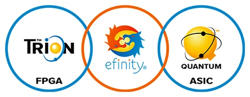 Figure 1: With their power-performance-area advantage, Trion FPGAs address applications such as custom logic, compute acceleration, ML, deep learning, and image processing. With the Efinity IDE, users can migrate seamlessly from a Trion FPGA to a Quantum ASIC for ultra-high volume production. (Image source: Efinix)
What is Quantum technology?
Like traditional FPGAs, Trion FPGAs include memory and DSP blocks. The difference lies in the programmable fabric (Figure 2). At the core of programmable logic is the logic element (LE). Each LE includes a look-up table (LUT), a multiplexer, and a register, all of which may be configured as required. In the case of traditional FPGAs, their programmable fabric may be described as “coarse-grained.”
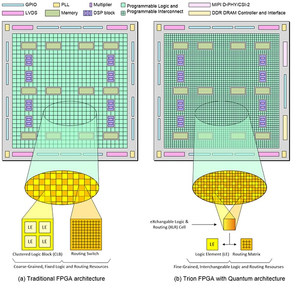 Figure 2: A traditional FPGA architecture (a) is coarse-grained, and although the logic and interconnect are programmable, they are still fixed resources. By comparison, Trion FPGAs (b) based on Quantum architecture are fine-grained, and their logic and routing resources are interchangeable (Image source: Max Maxfield)
In coarse-grained fabrics, multiple LEs are gathered together into a larger clustered logic block (CLB). Note that some vendors use the term configurable logic block (CLB), while others use logic array block (LAB), but they all mean the same thing.
It’s important to note that this illustration is an abstraction. The CLBs and routing switches (programmable interconnect) in traditional FPGAs are not really presented in a checkerboard pattern as shown here. However, they are fixed and immutable in that programmable logic will always be programmable logic, and programmable interconnect will always be programmable interconnect.
Compared to traditional architectures, Trion FPGAs are much finer grained, down to the resolution of a single logic element. Furthermore, each exchangeable logic and routing (XLR) cell can be configured to act as an LE or as part of the routing matrix.
The configuration cells used in Quantum architecture are SRAM based, which means this technology is “silicon agnostic”. They can be fabricated using any standard CMOS process without the need for special processing steps that are demanded by alternative configuration technologies, like flash and antifuse, that are used in some mid-range FPGAs.
It is this software-configurable logic and routing and high-performance adaptive interconnect that gives the Quantum-based approach a 4x improvement in terms of power-performance-area (PPA) compared to traditional SRAM-based FPGAs created at the same process technology node.
Also, FPGAs created using the Quantum architecture require only seven metallization layers, as opposed to the 12+ demanded by traditional FPGAs. Since each additional layer of metal requires multiple mask and process steps, using only seven layers reduces design and manufacturing costs and increases yield.
All these characteristics and features are very useful for designers looking for cost, size, performance, and flexibility advantages for edge computing and image processing. As such, Trion FPGAs are ideally suited to both traditional FPGA applications and to emerging edge computing and image processing applications. The latter include mobile, Internet of Things (IoT), automation, robotics, sensor fusion, computer vision, AI, and ML.
The structure of Trion FPGAs
Trion FPGAs are manufactured on a 40 nanometer (nm) low power silicon process with between four thousand (K) and 200K LEs, though the process is scalable to much larger devices. All Trion FPGAs include memory and DSP blocks, but their capacity and number vary depending on the size of the device. Smaller devices like the T4F81C2 are more minimalistic in their features (i.e., 3,888 LEs, 78,848 memory bits, 59 GPIOs) and are targeted at handheld, control plane functions.
Higher end devices like the T20F256C3 contain correspondingly more resources (i.e., 19,728 LEs, 1,069,548 memory bits, 195 GPIOs). The T13F256C3 is similar to the T20F256C3, but has 12,828 LEs. Also, devices like the T13/T20 come in different versions (Figure 3).
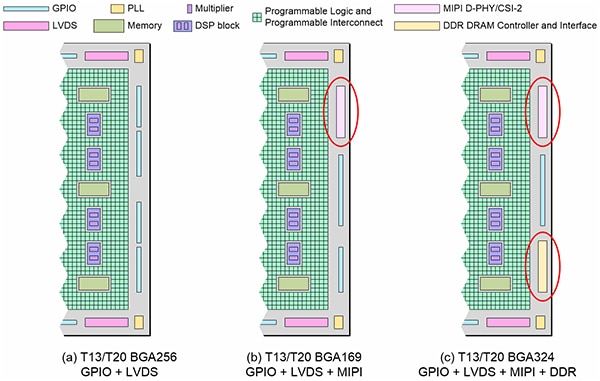 Figure 3: The Efinix T13/T20 BGA256s (a) are a generic FPGA that are a good choice for designs with I/O intensive needs; the T13/T20 BGA169s (b) include two MIPI D-PHY/CSI-2 hard core blocks for designs that need to support the MIPI camera interface; and the T13/T20 BGA324s (c) augment the MIPI interfaces with a hard core x16-bit double data rate (DDR) DRAM interface and controller for designs with memory bandwidth intensive needs. (Image source: Max Maxfield)
MIPI CSI-2 is the most widely used camera interface in mobile and other markets due to its low power, low latency, and low-cost chip-to-chip connectivity. It also supports a broad range of high-performance formats, including 1080p, 4K, 8K (and higher) video, as well as high-resolution imaging. Of particular interest here is the fact that MIPI CSI-2 is the predominant interface used for vision sensors in edge applications. To support designs for these applications, the T13/T20 BGA169s FPGAs include two MIPI D-PHY/CSI-2 hard core blocks (Figure 3, again).
DDR memory supports high bandwidth data transfers, but it also requires adherence to a strict timing protocol. In addition to hardened MIPI D-PHY/CSI-2 interfaces, the Trion T13/T20 BGA324s (Figure 3, again) also include a hardened x16-bit DDR DRAM interface and controller for designs with memory bandwidth intensive needs.
Quantum ASICs
As was previously noted, the configuration cells used in Trion FPGAs are SRAM based. As a result, when the system is first powered up, Trion FPGAs need to have their configuration data loaded, either from an external memory device or by “bit-banging” via the host processor. To do this in ultra-high volume production, Efinix also offers Quantum Accelerated embedded FPGA (eFPGA) solutions in the form of Quantum ASICs. In this case, Efinix can take T4, T8, T13, or T20 designs and create mask programmed Quantum ASIC versions that boot internally without the need for an external configuration device.
Design and development with Trion FPGAs
Efinix offers a variety of evaluation boards and development kits to allow users to become familiar with Trion FPGAs. These include the Trion T8F81C-DK T8 Trion FPGA development kit, the Trion T20F256C-DK T20 Trion FPGA evaluation board, and the Trion T20MIPI-DK T20 MIPI D-PHY/CSI-2 development kit.
One of the most common techniques used to develop with FPGAs is called language-driven design (LDD). This involves capturing the design intent at a level of abstraction known as register transfer level (RTL) using a hardware description language (HDL) such as Verilog or VHDL. Following verification via logic simulation, this representation is then fed into a synthesis engine, along with additional information such as the target FPGA type, pin assignments, and timing constraints, such as maximum input-to-output delays. The output from the synthesis engine is a configuration file which is loaded directly into the FPGA or into an external memory device (Figure 4).
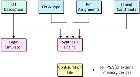 Figure 4: Following verification via logic simulation, the RTL design description is fed into a synthesis engine along with additional design details like the FPGA type, pin assignments, and timing constraints. The output from the synthesis engine is a configuration file which is loaded into the FPGA. (Image source: Max Maxfield)
Efinix’s Efinity IDE falls into this class of tool. This software provides a complete RTL-to-bitstream flow with a simple, easy-to-use graphical user interface (GUI) and command line scripting support. An intuitive dashboard guides the developer through the flow (i.e., synthesis, placement, routing, bitstream generation), where each stage can be controlled automatically or manually. Developers can use Efinity’s synthesis engine to take full advantage of the Quantum architecture featured in Trion FPGAs to generate devices with the promised 4x PPA improvements.
In addition to supporting simulation flows using the ModelSim, NCSim, or free IVerilog simulators, the Efinity IDE also features an Interface Designer to constrain logic and assign pins to blocks in the device periphery, a Floorplan Editor to browse through a design's logic and routing placement, a Timing Browser and static timing analysis to measure a design's performance, and an integrated hardware Debugger with Logic Analyzer and Virtual I/O debug cores.
Conclusion
As designers perform more image, AI, and ML processing at the edge, instead of, or to complement a cloud-based approach, they need to consider FPGAs as part of their processing architecture to better address issues such as cost, performance, power consumption, size, scalability, flexibility, and upgradability.
For some designers, this may involve a learning curve; but as shown, advances in FPGAs such as Efinix’s Quantum technology can quickly make the investment worthwhile through lower cost, smaller form factors, higher performance, and greater flexibility.
As a result, FPGAs are now ideally suited for both traditional FPGA applications as well as for emerging edge computing for mobile, IoT, automation, robotics, sensor fusion, computer vision, AI, and ML applications.
Additional Resources
- Fundamentals: The IoT, IIoT, AIoT, and Why They’re the Future of Industrial Automation
- Fundamentals of FPGAs: What Are FPGAs and Why Are They Needed?
- Fundamentals of FPGAs – Part 2: Getting Started with Lattice Semiconductor’s FPGAs
- Fundamentals of FPGAs – Part 3: Getting Started with Microchip Technology’s FPGAs

Disclaimer: The opinions, beliefs, and viewpoints expressed by the various authors and/or forum participants on this website do not necessarily reflect the opinions, beliefs, and viewpoints of DigiKey or official policies of DigiKey.


