Why and How to Use Efinix FPGAs for AI/ML Imaging — Part 1: Getting Started
Contributed By DigiKey's European Editors
2023-04-20
Editor’s Note: New approaches to FPGA architectures bring finer-grained control and greater flexibility to address the needs of machine learning (ML) and artificial intelligence (AI). Part 1 of this two-part series introduces one such architecture from Efinix and how to get started with it using a development board. Part 2 discusses interfacing the development board to external devices and peripherals, such as a camera.
FPGAs play a critical role in many applications, from industrial control and safety to robotics, aerospace, and automotive. Thanks to the flexible nature of the programmable logic core and their wide interfacing capabilities, one growing use case for FPGAs is in image processing when ML inference is to be deployed. FPGAs are ideal for implementing solutions that have several high-speed camera interfaces. In addition, FPGAs also enable the implementation of dedicated processing pipelines in the logic, thereby removing bottlenecks that would be associated with CPU or GPU-based solutions.
For many developers, however, their applications require more ML/AI functionality and finer-grained control or routing and logic, beyond what classic FPGA architectures with combinatorial logic blocks (CLBs) can provide. Newer approaches to FPGA architectures address these issues. For example, Efinix’s Quantum architecture uses an eXchangeable Logic and Routing (XLR) block.
This article discusses key features and attributes of the Efinix FPGA architecture, emphasizing its AI/ML capabilities and introducing real-world implementations. It then discusses a development board and associated tools that developers can use to quickly get started on their next AI/ML imaging design.
Efinix FPGA devices
Efinix currently offers two device ranges. It initially introduced the Trion family, which offers logic densities from 4000 (4K) to 120K logic elements (LEs), and is fabricated using an SMIC 40LL process. The newest line of devices, the Titanium family, offers logic densities from 35K to 1 million (1M) logic elements, and is fabricated on the very popular TSMC 16 nanometer (nm) node.
Both offerings are based around the Quantum architecture, which is unique in the FPGA world. The standard FPGA architecture is based on CLBs which, at the simplest level, contain a look-up table (LUT) and flip-flops. The CLBs implement logic equations that are then interconnected via routing. Efinix’s Quantum architecture moves away from distinct logic and routing blocks with the XLR block.
What makes an XLR block unique is that it can be configured to function as a logic cell with an LUT, a register and adder, or a routing matrix. This approach offers a finer-grained architecture that provides routing flexibility, enabling implementations that are logic heavy or routing heavy to achieve the desired performance.
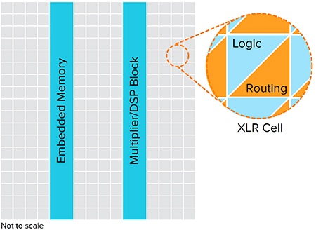 Figure 1: What makes an XLR block unique is that it can be configured to function as either a logic cell with an LUT, a register and adder, or a routing matrix. (Image source: Efinix)
As the newest family, the Titanium devices offer the most advanced features for the developer (Figure 2). Along with the XLR core, they provide multi-gigabit serial links which operate at either 16 gigabits per second (Gbps) or 25.8 Gbps, depending on the device selected. These multi-gigabit links are crucial for enabling high-speed data transfer on and off the chip.
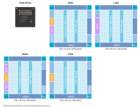 Figure 2: The Titanium FPGA Ti180 comes in a variety of options depending on the bus width, I/O, and memory requirements. (Image source: Efinix)
Titanium devices also provide a wide range of input/output (I/O) interfacing capabilities that can be grouped as general purpose I/O (GPIO), and that can support single-ended I/O standards such as low-voltage CMOS (LVCMOS) at 3.3 volts, 2.5 volts, and 1.8 volts.
For high-speed and differential interfacing, the Titanium devices provide high-speed I/O (HSIO) which supports single-ended I/O standards such as LVCMOS at 1.2 volts, 1.5 volts, and SSTL and HSTL. Differential I/O standards supported by HSIO include low-voltage differential signaling (LVDS), differential SSTL, and HSTL.
Modern FPGAs also require closely coupled, high-bandwidth memory, which is used to store image frames for image processing applications, sample data for signal processing, and of course, to run operating systems and software for processors implemented within the FPGA. The Titanium range of devices provides the ability to interface with dynamic data rate four (DDR4) and low-power DDR4(x) (LPDDR4(x)). Depending on the exact Titanium device selected, the bus width support is x32 (J) or x16 (M), while some devices have no LPDDR4 support (L).
Titanium FPGAs are SRAM based and require a configuration memory, with the device configuration performed by either master/slave Serial Peripheral Interconnect (SPI) or JTAG. To ensure this configuration method is secure, the Titanium FPGA uses AES GCM encryption of the bitstream, along with AES GCM and RSA-4096 to provide bitstream authentication. Strong security like this is required since FPGAs are deployed at the edge where malicious actors could access and manipulate their behavior.
Development board introduction
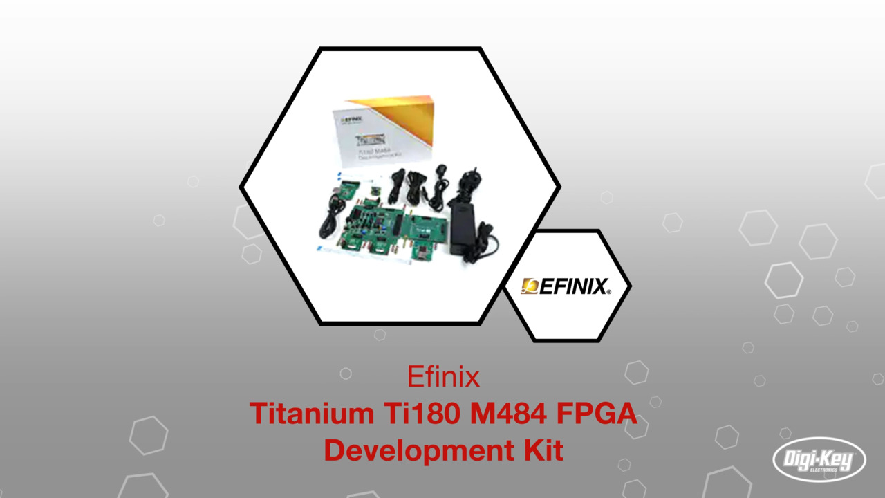
Development boards form a critical element of the FPGA evaluation process since they can be used to explore the capabilities of a device and prototype applications, thereby helping to reduce overall risk. The first development board available to evaluate Titanium FPGAs and begin prototyping applications is the Ti180 M484 (Figure 3). The board features an FPGA Mezzanine Card (FMC) connector and four Samtec QSE connectors.
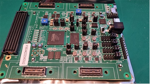 Figure 3: Along with a Titanium FPGA, the Ti180 M484 development kit features an FMC connector and four Samtec QSE connectors. (Image source: Adam Taylor)
The Ti180 FPGA fitted to this development board provides 172K XLR cells, 32 global clocks, 640 digital signal processing (DSP) elements, and 13 megabits (Mbits) of embedded RAM. The DSP elements provide the ability to implement fixed point 18 x 19 multiplications and 48-bit multiplications. This DSP can also be optimized for single instruction, multiple data (SIMD) operations running in either a dual or quad configuration. DSP elements can also be configured to perform floating point operations.
Like most development boards, the Ti180 development board provides simple LEDs and buttons. Its real power, however, comes in its interfacing capabilities. The Ti180 development board provides a low-pin-count FMC connector that enables a wide range of peripherals to be connected. As it’s a widely used standard, there are many FMC cards that enable interfacing of high-speed analog-to-digital converter (ADC), digital-to-analog converter (DAC), networking, and memory/storage solutions.
In addition to the FMC connection, the board provides four Samtec QSE connectors which enable the developer to add expansion cards. These QSE connectors are used to provide MIPI inputs and outputs, with each QSE connector providing either a MIPI input or output.
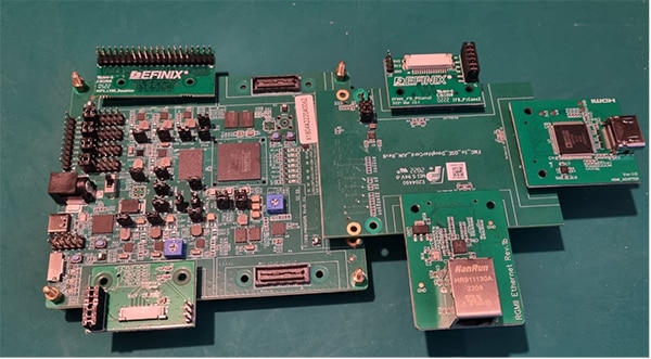 Figure 4: The Ti180 M484 development kit is shown with its versatile range of expansion options based on QSE and FMC connectors. (Image source: Adam Taylor)
The Ti180 board also provides 256 Mbits of LPDDR4 to support the high-performance memory required in image or signal processing applications. In addition, the development board provides a range of clocking options at 25, 33.33, 50, and 74.25 megahertz (MHz), which can be used with the device phase lock loop (PLL) to generate different internal frequencies.
The ability to reprogram and debug live on the board during development is critical and requires a JTAG connection, which is provided on-board via a USB-C interface. Also provided is non-volatile memory in the form of two, 256-Mbit NOR flash devices that can be used to demonstrate the configuration solution.
The board is powered from a 12-volt universal power adaptor that is included in the box. Also included is an FMC-to-QSE break out, along with QSE-based expansion cards for HDMI, Ethernet, MIPI, and LVDS. To demonstrate the Ti180 image processing capabilities, a dual RPI daughter card and two IMX477 camera cards are also provided.
The software environment
Implementing designs targeting the Ti180 development board use the Efinix software Efinity. The software enables the generation of a bit stream via synthesis and place and route. It also provides developers with intellectual property (IP) blocks, timing analysis, and on-chip debugging.
Note that a development board is required to gain access to the Efinity software. Unlike other vendors, though, the tool does not have different versions that require additional licensing.
Within Efinity, new projects are created targeting the selected device. RTL files can then be added to the project, and constraints created for timing and I/O design. It’s within Efinity that developers are also able to implement the I/O design, utilizing the HSIO, GPIO, and specialized I/O.
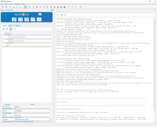 Figure 5: Within Efinity, new projects are created targeting the selected device. (Image source: Adam Taylor)
A critical element of FPGA design is leveraging IP, especially for complex IP such as AXI interconnects, memory controllers, and softcore processors. Efinity provides developers with a range of IP blocks that can be used to accelerate the design process.
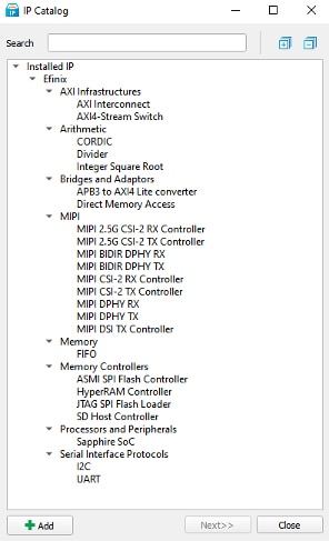 Figure 6: Efinity provides developers with an IP catalog that they can use to accelerate the design process. (Image source: Adam Taylor)
While FPGAs are excellent at implementing parallel processing structures, many FPGA designs include softcore processors. These provide the ability to implement sequential processing, such as network communications. To enable the deployment of the softcore processors in the Efinix devices, Efinity provides the Sapphire system-on-chip (SoC) configuration tool. Sapphire allows the developer to define a multi-processor system that has both caches and cache coherency across multiple processors, along with the ability to run an embedded Linux operating system. Within Sapphire, the developer can choose between one and four softcore processors.
The softcore processor being implemented is the VexRiscV soft CPU, which is based on the RISC-V instruction set architecture. The VexRiscV processor is a 32-bit implementation which has extensions for pipelining and offers a configurable feature set, making it ideal for implementation in Efinix devices. Optional configurations include a multiplier, atomic instructions, floating point extensions, and compressed instructions. Depending on the configuration of the SoC system, performance will range between 0.86 and 1.05 DMIPS/MHz.
Once the hardware environment has been designed and implemented in the Efinix device, the application software can be developed using the Ashling RiscFree IDE. Ashling RiscFree is an Eclipse-based IDE that enables the creation and compilation of application software, along with debug on the target to fine-tune the application prior to deployment.
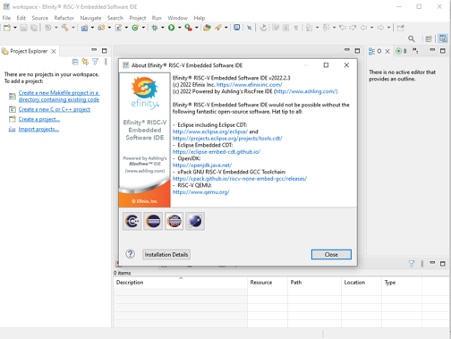 Figure 7: Ashling RiscFree is an Eclipse-based IDE that enables the creation and compilation of application software, along with debug on the target. (Image source: Adam Taylor)
If an embedded Linux solution is being developed, all necessary boot artifacts are provided, including First Stage Boot Loader, OpenSBI, U-Boot, and Linux using Buildroot. Alternatively, the developer can use FreeRTOS if a real-time solution is required.
AI implementation
Building upon the RISC-V softcore operation is Efinix’s AI implementation. This leverages the custom instruction capability of the RISC-V processor to enable the acceleration of TensorFlow Lite solutions. The use of the RISC-V processor also enables users to create custom instructions that can be used as part of the pre-processing or post-processing following the AI inference, creating a more responsive and deterministic solution.
To get started on an AI implementation, the first step is to explore the Efinix model zoo, which is a library of AI/ML models optimized for its end technology. For developers working with the Efinix devices, the model zoo can be accessed, and the network trained using Jupyter Notebooks or Google Colab. Once the network has been trained, it can be converted from a floating point model to a quantized one using the TensorFlow Lite convertor.
Once in the TensorFlow Lite format, Efinix’s tinyML accelerator can be used to create a deployable solution on the RISC-V solution. The tinyML generator enables the developer to customize the accelerator implementation and generate the project files. When deployed in this manner, the acceleration can range between 4x and 200x depending upon the selected architecture and customization.
Conclusion
Efinix devices provide developers with flexibility thanks to their unique XLR architecture. The toolchain provides the ability to not only implement RTL design, but also implement complex SoC solutions that deploy softcore RISC-V processors. Building on top of the softcore SoC is an AI/ML solution that enables the deployment of ML inference.

Disclaimer: The opinions, beliefs, and viewpoints expressed by the various authors and/or forum participants on this website do not necessarily reflect the opinions, beliefs, and viewpoints of DigiKey or official policies of DigiKey.


