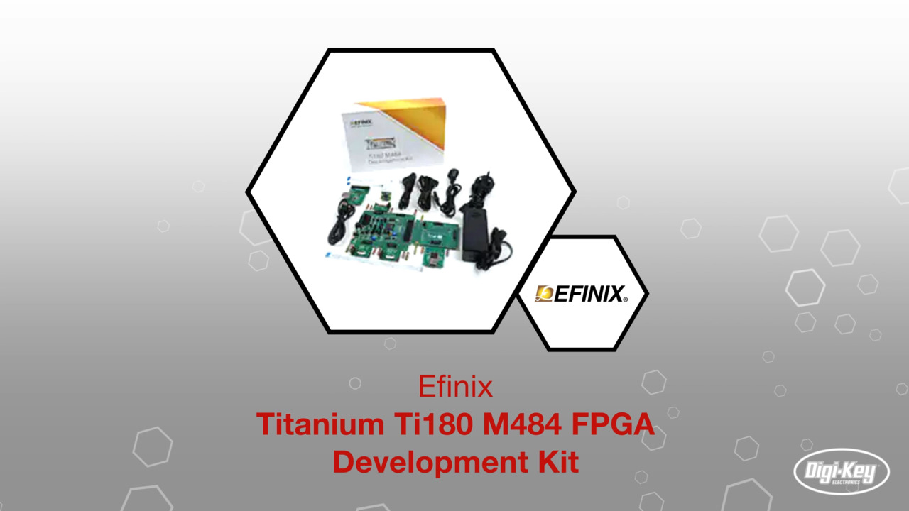
Why and How to Use Efinix FPGAs for AI/ML Imaging Part 2: Image Capture and Processing
Contributed By DigiKey's European Editors
2023-05-05
Editor’s Note: New approaches to FPGA architectures bring finer-grained control and greater flexibility to address the needs of machine learning (ML) and artificial intelligence (AI). Part 1 of this two-part series introduces one such architecture from Efinix and how to get started with it using a development board. Here, Part 2 discusses interfacing the development board to external devices and peripherals such as a camera, and how to leverage the FPGA to remove image processing bottlenecks.
FPGAs play a critical role in many applications, from industrial control and safety to robotics, aerospace, and automotive. Thanks to the flexible nature of the programmable logic core and their wide interfacing capabilities, one growing use case for FPGAs is in image processing, where machine learning (ML) can be deployed. FPGAs are ideal for implementing solutions that have several high-speed camera interfaces thanks to their parallel logic structure. In addition, FPGAs also enable the use of a dedicated processing pipeline in the logic, thereby removing shared-resource bottlenecks that would be associated with CPU or GPU-based solutions.
This second look at Efinix’s Titanium FPGAs will examine the reference image processing application that comes with the FPGA’s Ti180 M484 development board. The aim is to understand the constituent parts of the design, and to identify where FPGA technology enables the removal of bottlenecks or enables other benefits to developers.
The Ti180 M484-based reference design
Conceptually, the reference design (Figure 1) receives images from several Mobile Industry Processor Interface (MIPI) cameras, performs frame buffering in the LPDDR4x, and then outputs the images to a High Definition Multimedia Interface (HDMI) display. An FPGA Mezzanine Card (FMC) and four Samtec QSE interfaces on the board are used to provide the camera inputs and HDMI output.
 Figure 1: Conceptually, the Ti180 M484 reference design receives images from several MIPI cameras, performs frame buffering in the LPDDR4x, and then outputs the images to an HDMI display. >(Image source: Efinix)
The FMC to QSE expansion card is used in conjunction with the HDMI daughter card to provide the output video path, while three QSE connectors are used to interface with the DFRobot SEN0494 MIPI cameras. If multiple MIPI cameras are not available, a single camera can be used by looping back the single camera channel to simulate additional cameras.
At a high level, this application may appear to be straightforward. However, receiving multiple high-definition (HD) MIPI streams at a high frame rate is challenging. This is where FPGA technology is beneficial because it allows designers to utilize multiple MIPI streams in parallel.
The architecture of the reference design leverages both parallel and sequential processing structures with the FPGA. The parallel structures are used to implement the image processing pipeline, while a RISC-V processor provides the sequential processing used for the FPGA look-up tables (LUTs).
The image processing pipeline can be split into two elements within many FPGA-based image processing systems, namely the input and output streams. The input stream is connected to the camera/sensor interface, and processing functions are applied to the sensor’s output. These functions can include Bayer conversion, auto white balance, and other enhancements. In the output stream, the image is prepared for display. This includes changing color spaces (e.g., RGB to YUV) and post-processing for the desired output format, such as HDMI.
Often the input image processing chain operates at the sensor pixel clock rate. This has different timing to the output chain, which is processed at the output display frequency.
A frame buffer is used to connect the input to the output processing pipeline, which is often stored in external high-performance memory, such as LPDDR4x. This frame buffer decouples between the input and output pipelines, allowing access to the frame buffer via direct memory access at the appropriate clock frequency.
The Ti180 reference design uses a similar approach to the concepts outlined above. The input image processing pipeline implements a MIPI Camera Serial Interface 2 (CSI-2) receiver intellectual property (IP) core, which is built upon the MIPI physical layer (MIPI D-PHY)-capable input/output (I/O) of the Titanium FPGA. MIPI is a challenging interface because it uses both single-ended and differential signaling on the same differential pair, in addition to low-speed and high-speed communications. Integrating the MIPI D-PHY within the FPGA I/O reduces the complexity of the circuit card design while also reducing the bill of materials (BOM).
With the image stream from the camera received, the reference design then converts the output of the MIPI CSI-2 RX into an Advanced eXtensible Interface (AXI) Stream. An AXI Stream is a unidirectional high-speed interface that provides a stream of data from a master to a slave. Handshaking signals to transfer between a master and slave are provided (tvalid and tready) along with sideband signals. These sideband signals can be used to convey image timing information such as start of frame and end of line.
AXI Stream is ideal for image processing applications and enables Efinix to provide a range of image processing IP which can then be easily integrated into the processing chain as required by the application.
After being received, the MIPI CSI-2 image data and timing signals are converted into an AXI Stream and input into a direct memory access (DMA) module, which writes the image frame to the LPDDR4x and acts as the frame buffer.
This DMA module is operating under the control of the RISC-V core in the FPGA within a Sapphire system on chip (SoC). This SoC provides control, such as stopping and starting DMA writes, in addition to providing the DMA write channel with the necessary information to correctly write the image data to the LPDDR4x. This includes information on the memory location and the width and height of the image defined in bytes.
The output channel in the reference design reads the image information from the LPDDR4x frame buffer under the control of the RISC-V SoC. The data is output from the DMA IP as an AXI Stream, which is then converted from RAW format provided by the sensor to RGB format (Figure 2), and prepared for output over the on-board Analog Devices’ ADV7511 HDMI transmitter.
 Figure 2: Sample images output from the reference design. (Image source: Adam Taylor)
The use of the DMA also enables the Sapphire SoC RISC-V to access the images stored within the frame buffer, and the abstract statistics and image information. The Sapphire SoC is also able to write overlays into the LPDDR4x so that they can be merged with the output video stream.
Modern CMOS image sensors (CISs) have several modes of operation and can be configured to provide on-chip processing, and several different output formats and clocking schemes. This configuration is normally provided over an I²C interface. In the Efinix reference design, this I²C communication to the MIPI cameras is provided by the Sapphire SoC RISC-V processor.
Integration of the RISC-V processor within the Titanium FPGA reduces the overall size of the final solution as it removes the need to implement both complex FPGA state machines that increase design risk, as well as external processors that add to the BOM.
Inclusion of the processor also enables support with additional IP to communicate with the MicroSD card. This enables real-world applications where images may be required to be stored for later analysis.
Overall, the architecture of the Ti180 reference design is optimized to enable a compact, low-cost, yet high-performance solution that allows developers to reduce BOM cost through system integration.
One of the key benefits of reference designs is that they can be used to kickstart application development on custom hardware, enabling developers to take critical elements of the design and build off it with their needed customizations. This includes the ability to use Efinix’s TinyML flow to implement vision-based TinyML applications running on the FPGA. This can leverage both the parallel nature of FPGA logic and the ability to easily add custom instructions into RISC-V processors, allowing the creation of accelerators within the FPGA logic.
Implementation
As discussed in Part 1, the Efinix architecture is unique in that it uses eXchangeable Logic and Routing (XLR) cells to provide both routing and logic functionality. A video system such as the reference design is a mixed one that is both logic and routing heavy: extensive logic is required to implement the image processing features, and extensive routing is needed to connect the IP cells at the required frequencies.
The reference design uses approximately 42% of the XLR cells within the device, leaving ample room for additions, including custom applications such as edge ML.
Usage of the block RAM and digital signal processing (DSP) blocks is also very efficient, using only 4 of the 640 DSP blocks and 40% of the memory blocks (Figure 3).
|
Figure 3: Resource allocation on the Efinix architecture shows only 42% of the XLR cells are used, leaving ample room for additional processes. (Image source: Adam Taylor)
At the device IO, the DDR interface for the LPDDR4x is used to provide the application memory for the Sapphire SoC and the image frame buffers. All of the device-dedicated MIPI resources are utilized along with 50% of the phase lock loops (Figure 4).
|
Figure 4: Snapshot of the interface and I/O resources used. (Image source: Adam Taylor)
The general purpose I/O (GPIO) is used to provide the I²C communications along with several of the interfaces connected to the Sapphire SoC, including NOR FLASH, USB UART, and SD card. The HSIO is used to provide the high-speed video output to the ADC7511 HDMI transmitter.
One of the crucial elements when designing with FPGAs is not only implementing and fitting the design within the FPGA, but also being able to place the logic design within the FPGA and achieve the required timing performance when routed.
Long gone are the days of single-clock-domain FPGA designs. There are several different clocks, all running at high frequencies in the Ti180 reference design. The final timing table shows the maximum frequencies achieved for the clocks within the system. This is where the requested timing performance can also be seen in the constraints (Figure 5), which have a maximum clock frequency of 148.5 megahertz (MHz) for the HDMI output clock.
 Figure 5: Clock constraints for the reference design. (Image source: Adam Taylor)
Timing implementation against the constraints shows the potential of the Titanium FPGA XLR structure as it reduces the possible routing delay, thereby increasing design performance (Figure 6).
|
Figure 6: Timing implementation against the constraints shows the potential of the Titanium FPGA XLR structure to reduce the possible routing delay, thereby increasing design performance. (Image source: Adam Taylor)
Conclusion
The Ti180 M484 reference design clearly showcases the capabilities of Efinix FPGAs and the Ti180 in particular. The design leverages several of the unique I/O structures to implement a complex image processing path that supports several incoming MIPI streams. This image processing system operates under the control of a soft-core Sapphire SoC, which implements the necessary sequential processing elements of the application.
Disclaimer: The opinions, beliefs, and viewpoints expressed by the various authors and/or forum participants on this website do not necessarily reflect the opinions, beliefs, and viewpoints of DigiKey or official policies of DigiKey.