How to Improve Chiplet and WLCSP Assembly Yields Using Precision Tape and Reel Carriers
Contributed By DigiKey's North American Editors
2023-07-28
Industry standards like EIA-481 and International Electrotechnical Commission (IEC) 60286-3 mandate a maximum allowable camber of 1 millimeter (mm) over a 250 mm section of tape. They also set requirements for pocket sizes and overall dimensional tolerances. The standards don’t dictate specific materials for carrier tape systems. For small and rugged passive components like chip capacitors and resistors, a paper carrier tape can be a good choice. It’s inexpensive and can work well for components down to about 0.9 mm thick.
For thinner components that require a more rigid pocket, like many surface mount (SMD) semiconductor devices, polyester, polystyrene, or polycarbonate tapes can be a good choice. Polyester can experience a relatively high shrinkage, making the pockets less stable when stored for extended periods. Polystyrene tapes can have relatively high degrees of camber, yet still remain within the EIA-481 and IEC 60286-3 specifications. For the smallest components, like chiplets, WLCSPs, and BGAs, tapes made with engineered polycarbonate are often the best choice. Polycarbonate is strong and can protect delicate components from impact. Also, its low shrinkage keeps the pockets stable over longer periods. This helps to support the accurate tape feeding and pocket positions that are needed by pick-and-place machines.
Shrinking components
The continual shrinking of semiconductor devices is driving the need for tighter carrier tape dimensional tolerances. The standards for carrier tapes allow for pocket dimensions that can deviate up to 100 micrometers (μm). That’s okay for chip-style passive components and larger SMD semiconductor devices. Smaller components require tolerances of about 50 μm to prevent excessive device rotation or tilt in the pocket. The newest packages, like WLCSP, can require pockets that are 44% shallower, relative to larger devices (Figure 1). They also have tolerances of 30 μm which can only be consistently delivered using high-precision polycarbonate carrier tapes.
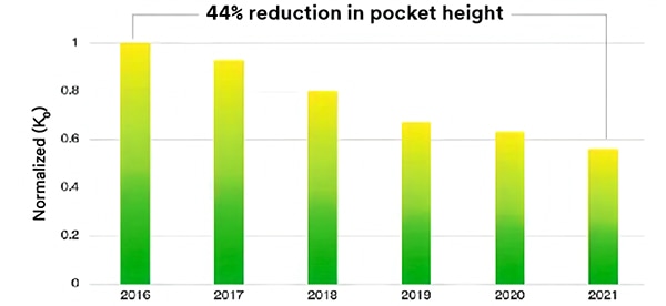 Figure 1: The use of smaller components such as WLCSP has resulted in a 44% reduction in the pocket heights of carrier tapes. (Image source: 3M)
The chiplet challenge
Using chiplets is one way that device makers are addressing the need for smaller solutions. Chiplets enable device designers to select from a catalog of chips that deliver specific functions that can be co-packaged to support higher system-level functionality. Common chiplet packaging technologies include 2.5 dimension (2.5D) and 3D structures. In 2.5D packaging, sometimes called interposer technology, several devices are mounted side-by-side on a single base. The interposer provides connectivity. In a 3D structure, the chips are stacked to achieve an even smaller footprint.
Chiplets are useful but require special handling. They also need to be protected from damage caused by ESD. Their small size makes them highly susceptible to misalignment and edge chipping in the pocket if the carrier tape is not highly stable with tight tolerances. In addition, their fabrication takes place in a class 10,000 cleanroom environment, and so they require suitable carrier tapes with specially engineered properties.
Polycarbonate properties
Engineered polycarbonate carrier tape has several properties that make it particularly suited for use with bare die, chiplet, WLCSP, and BGA devices. It has a nominal surface resistivity between 10⁴ ohms per square (Ω/square) and 10⁸ Ω/square. This enables it to dissipate charge accumulation due to triboelectric effects, and so protect ESD-sensitive devices. Polycarbonate is also very stable, experiencing typical shrinkage of <0.1% after 24 hours at +85°C, compared with <0.5% for polystyrene under the same conditions.
As an example, 3M’s 3000BD polycarbonate precision carrier tapes are made using an innovative process that produces highly precise and accurate pockets. Compared with the heat-formed pockets in conventional carriers, the 3000BD carriers have steeper sidewall angles that reduce the possibility of chip movement up the wall. They also have tight tolerances with respect to the length and width of the pocket to prevent component rotation, and have an extremely flat bottom that supports improved performance with pick-and-place equipment (Figure 2). In addition, the tight pocket tolerances protect against die edge chipping that can be a significant concern when shipping chiplets and bare die.
 Figure 2: Pockets in polycarbonate carrier tape (left) have steeper sides and flatter bottoms compared with alternative tapes (right). (Image source: 3M)
Polycarbonate carrier tape 3000BD is highly versatile and is offered in formats suitable for cleanroom and non-cleanroom environments. As it is cleaned and packaged in a class 10,000 cleanroom, it provides maximum protection from particle contamination with particle counts 60% to 70% lower than standard carrier tapes, and each plastic reel is sealed in a static shielding bag for protection. 3000BD carrier tapes are also available on cardboard reels for non-cleanroom applications and for less sensitive components.
These carrier tapes are made with a recyclable carbon-filled thermoplastic polymer film and support high levels of sustainability. They contain a lower level of corrosive, water-extractable ionic contaminants, compared with other carrier tapes, and meet the 5 parts per million (ppm) level needed to support improved solderability of tin-lead (SnPb), indium-lead (InPb), gold (Au) and copper (Cu) solder bumps (Figure 3).
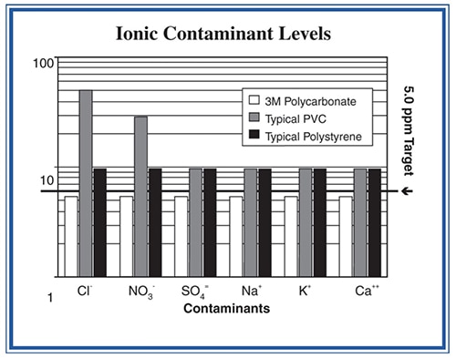 Figure 3: Comparison of ionic contamination levels in ppm for three carrier materials tested according to the requirements of MIL-STD-883E, Method 5011. (Image source: 3M)
Precision carriers
Two examples of the 3000BD series of polycarbonate precision carriers from 3M include the 3000BD-.12MM and the 3000BD-12X8, measuring 220 meters (m) long and 87 m long, respectively. They are offered as continuous, splice-free tapes measuring 8 mm wide to 44 mm wide, with a level winding format on plastic reel sizes ranging from 330 mm (13") to 560 mm (22") for cleanroom applications. A planetary winding format is available as a special order. Depending on variables like pocket depth and pitch and winding format, these reels will typically hold from 30 to 2,000 m of carrier tape (Figure 4).
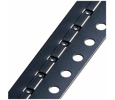 Figure 4: Polycarbonate precision carrier tape comes in rolls of up to 2,000 m. (Image source: 3M)
Cover tape choices
Selecting a high-performance, precision carrier tape is just half the answer. Designers also need a cover tape that can protect components and provide a smooth interface with pick-and-place equipment. Two common cover tape choices are heat-activated adhesive (HAA) and pressure-sensitive adhesive (PSA).
HAA tape is attached using a heated sealing shoe to press on the edges of the tape, thereby sealing in the components and leaving them free from adhesive residue. With HAA, the heat, pressure, and speed of sealing need to be accurately controlled. The adhesive on HAA tape can also be affected by temperature, humidity, and storage time. As a result, the peel force needed with HAA tape can be relatively inconsistent. The varying peeling force can result in devices popping out of the carrier pockets (called trampolining), slowing the assembly process.
For smaller components like chiplets and WLCSPs, PSA tape can be the better choice. PSA tapes have a smoother and more consistent peel force, minimizing trampolining and speeding the assembly process. Additionally, they are less sensitive to heat and temperature conditions and are less likely to vary over time. A drawback of some PSA tapes is that they may leave residue that can build up on assembly machines.
PSA tape seals in components
To complement the 3000BD series of polycarbonate precision carriers, designers can use 3M’s 2668 series of PSA conductive, high-shear, pressure-sensitive polyester film cover tapes. For example, the 2668-5.4MMX500M measures 5.4 mm wide by 300 m long, while the 2668-13.3MMX500M measures 13.3 mm wide by 300 m long. These cover tapes provide a flatter cover compared with HAA tapes, and provide a peel force with a variation of ±10 grams compared to ±20 grams for standard HAA cover tapes. They have a conductive blocker film layer next to the component to provide ESD protection and minimize adhesive residue.
Tape 2668 can be used with small components like bare die, chiplets, and WLCSPs that need extra care to prevent trampolining during the de-taping process (Figure 5). As a result, this tape can be used on high-speed de-taping equipment to speed the assembly process. It is available in standard and cleanroom compatible packaging. The differences between the two are:
- Standard tape comes on a plastic core, packaged with high-density paper wafer inserts and a centering core in a single polyethylene bag that is packaged in a cardboard carton.
- Cleanroom tape is the same tape, but is delivered in two polyethylene bags. This allows the cover tape to be used and stored in a cleanroom environment in the inner bag that has not had direct contact with the cardboard carton.
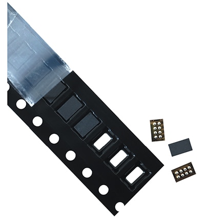 Figure 5: Shown is PSA carrier tape (upper left) peeling off a 3000BD conductive polycarbonate precision carrier with BGA devices for size reference. (Image source: 3M)
Conclusion
Precision polycarbonate carrier tape systems can be used together with PSA carrier tapes to improve yields when using bare die, chiplets, bumped die, chip-scale packaging, WLCSP, and BGA devices. These tape and reel systems provide extensive protection for delicate components and have the tight dimensional tolerances needed to support high-speed pick-and-place equipment.
Recommended reading

Disclaimer: The opinions, beliefs, and viewpoints expressed by the various authors and/or forum participants on this website do not necessarily reflect the opinions, beliefs, and viewpoints of DigiKey or official policies of DigiKey.


