Precision Thin Film Technology
2021-08-24
This article is intended to help circuit designers and component engineers improve their understanding of thin film technology. The article is a guide to understanding the use of thin film technology and the significant benefits it provides in reliability, size, and performance.
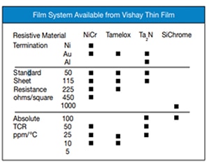 Figure 1: Thin film technologies available from Vishay. (Image source: Vishay)
Film types
Typically the films are sputtered onto a thickness of approximately 500 Angstroms. A selection of masks with a variation in line width and line spacing is used to manufacture the range of ohmic values. The sheet resistivity may also vary from 50 ohms per square to 2000 ohms per square. Each film has a specific purpose. As a general rule, the lower the sheet resistivity the better the overall electrical performance. Vishay is the only supplier and manufacturer of all film types.
Nichrome (NiCr) — The most popular of films has the best electrical specifications in terms of absolute TCR. Common sheet resistivities are 50, 100, and 200 ohms per square.
Tamelox — A proprietary alloy of Vishay Thin Film; combines the advantages of Nichrome and Tantalum Nitride that improves TCR linearity.
Tantalum Nitride (TaN2) — When deposited and processed correctly produces an alloy which is impervious to moisture. Electrical performance is not as good as Nichrome. Used in applications where the resistors experience low power (< 20%), no self-heating, and high relative humidity (80%).
Silicon Chrome (SiCr) — This material has a very high sheet resistivity (2000-3000) and is used to produce high resistances in a small area. Electrical specifications such as absolute TCR tracking, long-term stability, and voltage coefficients superior to thick film technology.
Passivation – SPM (Special Passivation Methods) now allows for enhanced passivation control under harsh environments conditioning (reference Tech Note SPM).
Thin film integrated construction
An integrated circuit is a grouping of elements which are formed and interconnected on a common substrate to form a functional network. An integrated resistor network is similarly defined as a grouping of resistive elements formed and interconnected on a common substrate. As in semiconductor fabrication, the elements are produced by deposition on, or reaction with, the substrate, and the patterns are produced by photolithographic imaging, followed by selective removal of unwanted materials. The resistors in a given network, being quite small and in close proximity, are exposed to nearly identical conditions during processing. Similarly, each network on the wafer or substrate is exposed to virtually the same conditions. Because several wafers are processed together, at the same time, and in the same equipment, uniformity is bestowed upon the entire lot — to hundreds or thousands of individual units. An added benefit of integrated construction is the integrity of the interconnections, which are inherently more reliable than individual connections between discrete components.
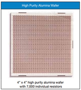 Figure 2: High purity alumina wafer showing thin film integrated construction. (Image source: Vishay)
Advantages of thin film integrated construction
- Extremely close matching of all elements in a network, ensuring close tracking over temperature and throughout life
- Very small, high-density, multi-element networks which save printed circuit board real estate
- Hermetic construction practical in a variety of standard contemporary formats
- Repeatable and consistent characteristics, part-to-part and lot-to-lot
- Very low inductance
- Outstanding reliability — fewer individual interconnections
- No thermoelectric effects
- Installed costs no more than discretes — often less
Interconnection reliability
Reliability studies by the military and other agencies have shown that — all other things being equal — the reliability of an assembly is directly proportional to the number of “man-made interconnections.” This is why the integrated circuit is more reliable than an assembly of discrete transistors, and the same applies to an integrated resistor network versus discretes. This is sometimes referred to as “inherent reliability.”
Resistance range
Thin film technology employs photolithographic precision patterning to give the designer a wide range of resistance values in the smallest possible area. This provides a choice of minimizing the size of the component or increasing the number of resistive elements in the same space. The total resistance achievable in a given area is dictated primarily by the sheet resistance of the film material and the patterning. In actual designs, however, the maximum area utilized is reduced because of space required for termination pads, internal conductors, special trimming features, and pin-out constraints.
Thin film resistive materials cover a normal sheet resistance range of 50 to 2000 ohms/square which results in an available resistance range for individual resistors from a few ohms to several megohms. The highest precision is normally found in the range 250 ohms to 100 kilohms.
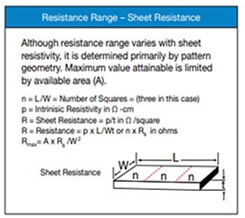 Figure 3: Resistance range is determined primarily by pattern geometry on the wafer sheet. (Image source: Vishay)
Very low resistance
When low resistance elements are incorporated in precision networks, the small but unavoidable resistances of the leads and conductive patterns on the chip and in the package must be taken into consideration. These lead effects can be minimized, but not completely eliminated, by proper design, processing, package selection, and assembly. However special attention must be given to the setting of specifications, particularly with regard to realistic tolerances on resistance and tracking, and to the method of their measurement.
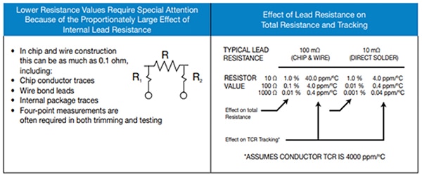 Figure 4: Internal lead resistance can have a large effect on total resistance values. (Image source: Vishay)
Resistance tolerance
Modern laser systems are capable of adjusting resistors to very close tolerances on either an absolute or relative basis: 0.01% and 0.005% respectively. Furthermore, the responsible manufacturer will actually “guard band” the trimming so that the internal specification will be tighter than the release specification.
The closer the required tolerance, the more carefully the resistor must be designed to achieve a tight distribution, well within the tolerance limits, and with a cost-effective trimming speed. One of the ways this is achieved is to provide special trimming geometries. These features reduce the sensitivity of the resistor to the amount of material being removed by the laser, allowing successively higher levels of accuracy to be obtained. These features utilize additional substrate area, which sometimes requires trade-offs between cost and performance. One of the features which distinguish modern thin film technology for use in precision networks is the electrical and mechanical stability of the films. This is important because closely trimmed resistors must endure the sometimes stressful conditions of assembly without significant drift. This again emphasizes the inherent advantages of integrated construction over individual discrete resistors, since any changes which do occur will be common to all resistors in the network, thus preserving the ratios precisely as trimmed.
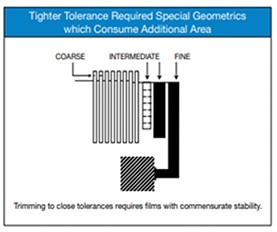 Figure 5: Tighter tolerance requirements can result in additional area being used. (Image source: Vishay)
Temperature coefficient of resistance (TCR)
The temperature coefficient of resistance is the measure of resistance change as a function of the ambient temperature. It is defined as the unit change of resistance per unit change in temperature and is commonly expressed as parts per million per centigrade degree (ppm/°C). It is the property by which resistors are most often characterized or differentiated. Historically, discrete resistors, including those made from films, were graded by lots according to TCR value. The relatively recent use of sputter deposition to control film composition, together with related improvements in processing, have resulted in the so-called “third-generation” thin film products with TCRs consistently less than 10 ppm/°C, absolute.
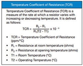 Figure 6: Temperature Coefficient of Resistance is a measure of the rate at which a resistor varies with increasing or decreasing temperature. (Image source: Vishay)
TCR is usually determined experimentally by measuring the resistance at several temperatures and calculating the rate of change over the appropriate temperature interval, e.g. +25°C to +125°C. If the resistance changes linearly with temperature, the TCR is a constant, regardless of the temperature interval. However, when it is not linear, as is the case for the commonly used nickel/chromium alloys, the TCR is expressed as the slope of the line connecting two points on the resistance vs. temperature curve, e.g. +25°C and +125°C. In other words, it is the average TCR over the interval. The more non-linear the relationship, the poorer the approximation of the average.
It is absolutely crucial in specifying TCR that the temperature interval be clearly specified as well.
The procedure outlined in MIL-STD-202 Method 304 is often referenced as a standard for measuring TCR. In this method, average TCRs are calculated for a series of intervals between +25°C and -55°C and between +25°C and +125°C. The highest value is recorded as the TCR. This reflects the full military operating range but may result in over-specification for components having a different or narrower operating temperature interval.
 Figure 7: Examples of TCRs for different resulting slopes. (Image source: Vishay)
Through an understanding of the effects of alloy composition and the ability to carefully control processing, it is possible to “tailor” the resistance vs. temperature curve to produce TCRs that are a) negative over the entire range, b) positive over the entire range, or c) negative in the low end, positive at the high end, with a relatively flat “zero TCR” sector in a range about room temperature. This can be used to advantage for equipment operating in the vicinity of room temperature or otherwise requiring temperature compensation.
Tracking
Most applications in which precision thin film networks are employed depend upon achieving and maintaining close relative resistance values. Thus, relative changes in resistance within a network, called “tracking”, are very important. Thin film networks excel at tracking. There are several different aspects of tracking which are important to understand and differentiate.
TCR Tracking — TCR tracking is defined as the difference between the TCRs of a pair of resistors over a given temperature interval. Achieving close TCR tracking in discrete resistors is difficult and places severe burdens on the manufacturing process to produce to a very close absolute TCR limit. By contrast, the integrated construction of thin film networks assures extremely close TCR tracking because the resistors are produced as a group under nearly identical process conditions. Moreover, the resistors are small and in close proximity on the surface of a common substrate of high thermal conductivity, which keeps them at or near the same temperature in operation.
Nevertheless, process and material variations can occur which produce small but measurable differences in the TCRs of neighboring resistors on the same wafer. Process variables which may affect this include non-uniform film deposition, substrate defects, thermal gradients during annealing, and non-uniform stresses. Design can also play a role. However, by employing state-of-the-art process controls, measuring equipment, and techniques, TCR tracking can be controlled to within a few tenths of a part per million, per degree, given the proper circuit and chip configuration and packaging.
A factor which results in the apparent TCR tracking being higher than the “true” tracking is the presence of a common tap lead having a measurable resistance (r).
![]()
where TCR (r) is the TCR of the common lead material, typically metallic. For example: a 1 kilohm resistor having a TCR of 8.9 ppm/°C connected to a 2-kilohm resistor with a TCR of 8.5 ppm/°C and a shared output lead of resistance 0.1 ohm with TCR (r) of 4000 ppm/°C will exhibit TCR tracking.

The extraneous contribution by the common lead (0.2 in the case above) disappears in the event that critical ratios are specified and measured according to voltage division rather than resistance ratio.
 Figure 8: Examples of tracking distributions for widely and closely spaced resistors. (Image source: Vishay)
 Figure 9: Rule of thumb for tracking integrated networks vs. discrete resistors. (Image source: Vishay)
Resistance tracking under power switching
Some circuits operate in a mode whereby current is switched off and on in one resistor, which is matched to a reference resistor carrying a constant current. In this case, even though the resistors may have identical TCRs and the substrate may be at a uniform ambient temperature, the resistances will differ in value as a result of self-heating. (Strictly speaking, this is not a true “tracking” requirement in as much as the resistors of interest are subjected to different stresses.) This difference will be governed by the absolute TCRs of the two resistors. In these applications, which are not uncommon, the resistors should have as low an absolute TCR as possible in the operating temperature region, and the resistors should be designed as close together as possible to minimize the temperature differences between them.
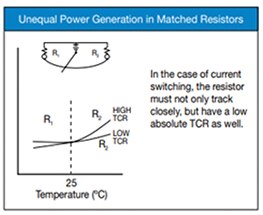 Figure 10: Example of unequal power generation in matched resistors. (Image source: Vishay)
Voltage ratios
Resistors are frequently employed as voltage dividers. In this case, and where precise tolerances are involved, it is more appropriate to deal with voltage ratios than with resistance ratios. There are three important aspects of voltage ratios that should be understood in comparison with resistance ratios. They are the voltage ratio itself, the tolerance of the voltage ratio, and voltage ratio tracking.
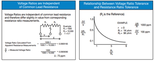 Figure 11: Voltage ratios are independent of common lead resistance. (Image source: Vishay)
Ideally, the voltage drop across a pair of resistors is determined by the ratio of resistance values: R1/(R1 + R2). When the resistance values are not equal, the voltage ratio will differ from that calculated from the apparent (measured) resistance values by an amount which is governed by the resistance of the common lead. This deviation can be quite significant, especially with low-value resistors.
For a 10-kilohm resistor in series with a 1 kilohm resistor, having a common “tap” lead with 100 milliohms resistance, the two ratios will differ by 75 ppm:

For a 1-kilohm resistor in series with a 100-ohm resistor, a 100-milliohm tap resistance will produce a difference in the respective ratios of more than 800 ppm.
This illustrates the importance of specifying the proper operating parameter.
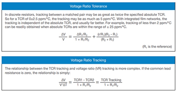 Figure 12: Voltage ratio tolerance and voltage ratio tracking equations. (Image source: Vishay)
However, when the common lead resistance (r) is measurable, the apparent TCR tracking is higher than the “true” tracking, as shown earlier, and the voltage ratio tracking is lower. The voltage ratio tracking is always less (better) than TCR tracking.
Stability
The effects described in the previous sections are reversible: the changes are not permanent and will disappear when the temperature returns to the starting point. There are, however, irreversible effects. As discussed earlier, most precision resistor networks are used in a ratio mode. They have been trimmed to tight tolerances and carefully engineered to track within these tight initial tolerances with regard to resistance or voltage ratios. But this is meaningless unless these tolerances can be preserved throughout the life of the network. This requires maximum film stability. Notably, recent advances in materials and processes have resulted in improving the stability of thin films to unprecedented levels, approaching those previously obtainable only with foils.
Extensive long-term stability testing of nickel/chromium alloys has shown conclusively that the rate of change of resistance with time is a single-valued function of substrate temperature. This is a mathematical way of stating that temperature is the only variable — whether it is induced by power loading or simply by the ambient. Moreover, it has been determined experimentally that the stability measured at a higher temperature may be confidently extrapolated to lower temperatures and longer times according to classical kinetic equations.
It is useful to think of the permanent changes in a pair of matched resistors as “stability tracking.” In contrast to TCR tracking, where close tracking is independent of the absolute TCR, stability tracking is somewhat dependent on the absolute stability. The more stable a pair of resistors, the less they will change in absolute value and in relationship to each other. Here again, the advantages of integrated construction are evident: all resistors in the network tend to have similar changes during life, and resistance ratios change far less than absolute values.
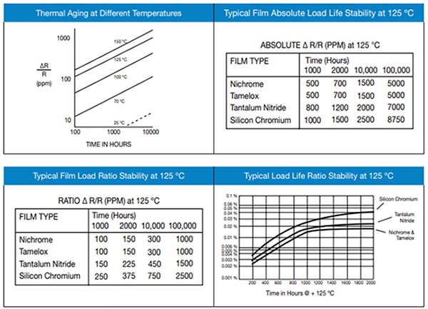 Figure 13: Stability is affected by the age of the components. (Image source: Vishay)
Power rating
Because thin film precision networks are not generally used in high-power applications, methods for establishing the maximum power ratings are not as critical as in general-purpose networks. However, limits must be set and this is best done by establishing upper temperatures limits.
Zero power temperature (sometimes called the maximum operating temperature) is the maximum temperature at which the part can be operated, for a specified time (usually 1000 hours), without excessive change (usually defined in relation to the initial tolerance), expressed in percent. For a thin film network required to maintain a 0.1 % tolerance, this zero power temperature would be +150°C. At this temperature, a resistor might exhibit a change on the order of 500 ppm absolute or 100 ppm relative to others in a network. If the maximum initial tolerance required were 0.01%, a more appropriate zero power temperature would be +125°C. These levels are for hermetically enclosed parts. If packaged non-hermetic, the parts would be given a lower temperature rating.
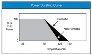 Figure 14: Typical power derating curve. (Image source: Vishay)
Full Power Rating — Rated power is generally accepted as that power which is required to raise the surface temperature of a part above some ambient temperature, usually +70°C, to the zero power temperature. This is expressed in watts-full power. A power derating curve is used to determine limits at intermediate temperatures.
Special consideration must be given to the rating of individual resistors within a network since the final surface temperature of an individual resistor will differ greatly depending upon whether other resistors in the network are under power. Although it is difficult to generalize, proper network design will account for these potential variations by arrangements providing uniform power density.
As indicated above, although the power levels in closer-tolerance precision networks are usually set lower, because chip dimensions are small, the power density can be high. A typical design level is 25 W/in2 for very precise networks, but thin films are capable of sustaining remarkably high levels of power density — as much as 200 W/in2 — without jeopardizing their integrity. As a final consideration, allowance must be made for the fact that packages vary widely in thermal resistance.
Voltage coefficient of resistance and current noise
These two characteristics, which may be quite a serious drawback in resistors made from composite materials such as cermets or polymers, can be generally ignored with thin film precision networks because the magnitudes are so small. This is one of the major advantages of monolithic thin film materials.
Voltage coefficient of resistance is the unit change in resistance per unit change in voltage expressed as ppm/volt. It is a measure of the non-ohmic behavior, and in thin films, reaches identifiable levels only in the megohm range, where it has been measured at about 0.1 ppm/V.
Current noise is characterized and measured using a standard instrument developed by the Quantek Company. For thin films, a typical value would be less than – 35 dB.
Thermoelectric effects
Thermoelectric voltages may be generated if the terminations of resistors are at different temperatures. This can be a significant problem with discrete resistors, where thermal gradients can exist over the relatively large dimensions. In thin film networks, all resistors are at or near the same temperature, as a result of their small size and the heat spreading effects of the thermally conducting substrate. Thermoelectric effects on thin films are typically < 0.1 µV/°C.
Frequency response of resistors
For frequencies greater than 100 MHz most resistors need to be considered in terms of an equivalent circuit with parasitic inductance and capacitance, see Figure 15. A typical impedance response is shown in Figure 16. The impedance response is dependent on the resistor size, trim method, part value, and termination style.
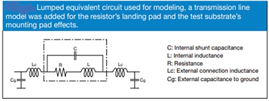 Figure 15: Most resistors need to be considered in terms of an equivalent circuit with parasitic inductance and capacitance for frequencies greater than 100 MHz. (Image source: Vishay)
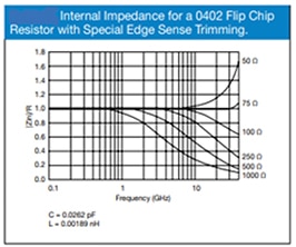 Figure 16: Typical internal impedance response for a 0402 flip chip resistor with special edge sense trimming. (Image source: Vishay)
Consideration of the size is of significant importance for reduction of parasitic impedance. The smaller the size the closer the part performs to an ideal resistor. Trim styles are also of importance.
Thin film resistors can be trimmed with various geometrical designs, see Figure 17. By maintaining a rectangular design-centered (balanced) between the contact pads versus other styles such as serpentine or L-trim the performance of the device can be improved.
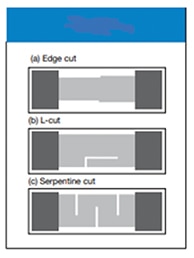 Figure 17: Thin film resistors can be trimmed with various geometrical designs. (Image source: Vishay)
See links below for Vishay thin film resistors
Leaded Network
Surface-mount chips
Through-hole
Disclaimer: The opinions, beliefs, and viewpoints expressed by the various authors and/or forum participants on this website do not necessarily reflect the opinions, beliefs, and viewpoints of DigiKey or official policies of DigiKey.


