How to Deliver Low-Noise, High-Density Power in a Small Form Factor for FPGAs and ASICs
Contributed By DigiKey's North American Editors
2023-04-06
Digital ICs with high-current requirements, such as FPGAs and ASICs, are increasingly at the center of embedded systems for applications such as automotive, medical, telecom, industrial, gaming, and consumer audio/video. Many of these applications are mission-critical such as automotive driver assistance systems (ADAS), and high reliability such as data centers.
In addition to the current requirements, these lower voltage devices have tight tolerance specifications for their power rails. Delivering this power with efficiency, accuracy, fast transient performance, stability, and low noise is critical to system performance and integrity.
Conventional switching regulator controllers and power subsystems have potential noise issues, both on their output rails and as radiated electromagnetic interference (EMI) and radio frequency interference (RFI), inadequate transient response, and layout limitations. To minimize noise, some applications use small and quiet low dropout (LDO) regulators that offer improved efficiency compared to earlier LDOs. Nonetheless, even these LDOs usually cannot meet system efficiency requirements, resulting in thermal dissipation concerns.
The efficient alternative to the LDO is the switching regulator, but these devices have inherently higher noise due to their clock and switching function. This noise needs to be mitigated if designers are to take full advantage of these switching devices.
Fortunately, there are new ways to balance noise versus efficiency. This article looks at recent innovations in the design of power conversion that have high efficiency and minimal space requirements, as well as greatly reduced switching regulator noise. It explores how innovative switching regulators can meet the multiple objectives for loads in the single-digit voltage, sub-10 ampere (A) range, and introduces the tiny Silent Switcher ICs in the LTC33xx family from Analog Devices as examples.
The current/voltage imperative
When transistors and ICs were invented and advanced in the second half of the 20th century, among their many virtues was that their per-function power requirements were very low in comparison to the vacuum tubes they replaced—easily by a factor of 100 or more. However, this advance soon led to higher densities of functions per device and circuit board, to the extent that ICs now require tens of amperes per rail, and often on multiple rails.
Among the ICs that require these high currents, which must ultimately dissipate the high amounts of associated power as heat, are field-programmable gate arrays (FPGAs) and application-specific ICs (ASICs). Both are widely used in embedded devices spanning the entire electronics industry, including automotive, medical, industrial, communications, gaming, and consumer audio/video devices.
The current needed by the FPGA or ASIC can be sourced via an AC/DC converter for line-powered devices or a DC/DC converter for battery-powered ones. In either case, a subsequent DC/DC step-down (buck) regulator is needed to provide and manage the single-digit rail voltage for the load at the needed current levels.
One way to provide the necessary power is to use a single DC/DC buck regulator to support all the circuit board devices and locate it off to the side or corner of the pc board to help manage heat dissipation issues and simplify the DC/DC system-level architecture.
However, this simple-sounding solution has its issues:
- First, there’s the unavoidable IR drop between the regulator and the loads due to the distance and high current levels (ΔV drop = load current I × trace resistance (R)). The solutions for this are to increase pc board trace width or thickness or use a stand-up busbar, but these use precious board real estate and add to the bill of materials (BOM).
- A technique to overcome IR drop is to use remote sensing of the voltage at the load, but this only works well for a single-point, non-dispersed load. It also brings new issues of potential oscillation, as the inductance of the longer supply rail and sensing leads can affect the transient performance of the regulator and the rails.
- Finally, and the issue that is often most difficult to manage, the longer power rails also are subject to more EMI/RFI noise pickup or are effective at radiating noise along their length, such that they act as antennas. The solution usually requires additional bypass capacitors, in-line ferrite beads, and other measures. Depending on its magnitude and frequency, this noise can adversely affect the reliable operation of the loads and make it challenging to meet the various regulatory mandates on noise emissions.
The noise versus efficiency conundrum
It is important to note that the “noise versus efficiency” conundrum for DC/DC regulators is a different scenario than the usual tradeoffs of engineering design. That situation is often about assessing tradeoffs and finding the “sweet spot” which balances favorable versus unfavorable attributes.
How is this situation different? Most tradeoff scenarios allow the designer to deliberately accept less of some desired parameter value in exchange for more of another one, moving along a continuum of tradeoffs (Figure 1, upper part).
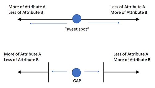 Figure 1: Most design situations allow the engineer to assess and then make various performance tradeoffs along a fairly continuous path (upper), but for the noise/efficiency of switching regulators versus LDOs, designs end up on either one side or the other, with little “middle ground” (lower). (Image source: Bill Schweber)
For example, the designer may choose an operational amplifier (op-amp) that draws more current (bad) in order to provide a higher slew rate (good) compared to another op-amp; a tradeoff is acceptable or necessary in the application.
However, with switching regulators and LDOs, their noise and efficiency attributes are largely “baked into” their structure. A designer cannot say, for example, that they will accept an LDO with 20% more noise in exchange for it offering an improvement of 10% in efficiency—that type of tradeoff does not exist. Instead, there is a gap in the attribute-tradeoff span (Figure 1, lower part).
Silent Switcher regulators resolve the tradeoff dilemma
An alternative and usually better solution is to use individual DC/DC regulators sited as close to their load ICs as possible. This minimizes IR drop, pc board footprint, and rail-noise pickup and radiation. However, for this approach to be viable, it’s essential to have small, efficient, low-noise regulators that can be placed next to the load and still meet all of its current requirements.
This is where the many Silent Switcher regulators are problem solvers. Not only do these regulators provide single-digit voltage outputs at current levels from a few amperes to 10 A, but they do so with extremely low noise, which is achieved by employing multiple design innovations.
These regulators shift the conventional thinking of the LDO versus switching-regulator gap with Silent Switcher 1 (first generation) and Silent Switcher 2 (second generation) devices. The designers of these devices identified the various noise sources and devised ways to attenuate each one.
Note that Silent Switcher regulators do not use the well-known and legitimate “spread-spectrum” technique of adding pseudorandom noise to the clock signal. This broadens the noise spectrum while reducing its amplitude at the clock frequency and its harmonics. While using spread-spectrum clocking can help meet regulatory limits, it does not reduce aggregate noise energy and may, in fact, put some noise in parts of the spectrum that affect circuit performance.
The benefits of the Silent Switcher 1 devices include low EMI, high efficiency, and a high switching frequency that moves much of the remaining noise away from parts of the spectrum where it would interfere with system operation or have regulatory issues. The Silent Switcher 2 benefits include all the features of Silent Switcher 1 technology plus integrated precision capacitors, a smaller solution size, and the elimination of sensitivity to the pc board layout.
Due to their tiny form factor (just a few millimeters (mm) square) and efficiency, these switchers can be located very close to the load FPGA or ASIC, thereby maximizing performance and eliminating uncertainties between datasheet performance specs and in-use reality. They change the “binary” dilemma of having to choose between accepting either more noise or less efficiency, allowing designers to have the best of both attributes when it comes to noise and efficiency.
How were these Silent Switcher benefits realized? It was done by taking a multifaceted approach:
- The main cause of noise in a switched-mode power supply is switched currents, not steady-state ones. In the topology of a conventional switching regulator, there is a current-flow path called a hot loop. This hot loop is not an independent current loop, but only a virtual current loop composed of the components of two real current loops (Figure 2).
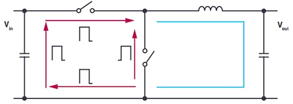 Figure 2: The usual switching regulator topology has a virtual current loop called a hot loop; it is composed of the components of two real current loops and has switched-current flows. (Image source: Analog Devices)
The Silent Switcher 2 technology from Analog Devices makes the critical hot loops as small as possible through the integration of input capacitors in the IC package. Also, by splitting the hot loop into two symmetrical shapes, two magnetic fields of opposite polarities are created and the radiated noise cancels itself out to a great extent.
- The second-generation architecture supports fast switching edges for high efficiency at high switching frequencies while simultaneously achieving good EMI performance. Internal ceramic capacitors on the DC input voltage (VIN) keep all the fast AC current loops small, improving EMI performance.
- The Silent Switcher architecture uses proprietary design and packaging techniques to maximize efficiency at very high frequencies and enable ultralow EMI performance, easily passing the CISPR 25 Class 5 peak EMI limits by using highly compact and robust designs.
- Active Voltage Positioning (AVP), a technique where the output voltage is dependent on load current, is used. At light loads, the output voltage is regulated above the nominal value, while at full load, the output voltage is regulated below the nominal value. The DC load regulation is adjusted to improve transient performance and reduce output capacitor requirements.
The many families of Silent Switcher
Silent Switcher regulators are available in many families and models, with different voltage/current ratings within each family. Some additional considerations vary from model to model, such as fixed versus adjustable output. Among the various members of the LTC33xx family are the:
- LTC3307: 5 volt, 3 A synchronous step-down Silent Switcher in a 2 mm × 2 mm LQFN package
- LTC3308A: 5 volt, 4 A synchronous step-down Silent Switcher in a 2 mm × 2 mm LQFN package
- LTC3309A: 5 volt, 6 A synchronous step-down Silent Switcher in a 2 mm × 2 mm LQFN package
- LTC3310: 5 volt, 10 A synchronous step-down Silent Switcher 2 in 3 mm × 3 mm LQFN package
Looking at the LTC3310 in more detail, this is a very small, low-noise, monolithic, step-down DC/DC converter that is capable of providing up to 10 A of output current from a 2.25 to 5.5-volt input supply; the VOUT range is 0.5 volts to VIN. Switching frequencies span 500 kilohertz (kHz) to as high as 5 megahertz (MHz). It requires only a few external passive components and has an efficiency of around 90% over most of its output load range (Figure 3).
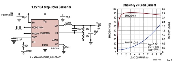 Figure 3: The LTC3310 step-down DC/DC regulator requires external active components and offers high efficiency over most of its load range. (Image source: Analog Devices)
It is available in four basic versions. The devices provide both low EMI and high efficiency at switching frequencies as high as 5 MHz, and there are versions of the LTC3310 family which are AEC-Q100 automotive qualified. Note that both first-generation (SS1) devices—LTC3310—and second-generation (SS2) devices—LTC3310S and LTC3310S-1—are available as adjustable output and fixed output devices (Table 1):
|
Table 1: The LTC3310 is offered in four basic versions, representing first and second-generation designs, as well as fixed and adjustable outputs. (Image source: Analog Devices)
For the adjustable versions, the output voltage is hard-programmed via a resistor divider between the output and the feedback (FB) pin using a simple equation to determine the correct resistor value (Figure 5).
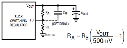 Figure 5: Establishing the output voltage of the adjustable LTC3310 devices requires only a basic resistor divider network based on a simple equation. (Image source: Analog Devices)
Noise levels are typically in the tens of microvolts. Two key metrics of the low-noise performance of the LTC3310 devices are the noise tests conducted in accordance with the relevant CISPR25 Class 5 peak limits. These include conducted noise (Figure 6) and radiated noise in both horizontal and vertical planes (Figure 7).
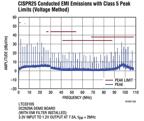 Figure 6: A properly arranged regulator based on the LTC3310S meets the stringent CISPR25 conducted EMI emissions (with Class 5 peak) limits. (Image source: Analog Devices)
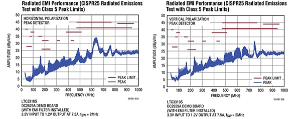 Figure 7: For radiated emissions tests, the LTC3310S meets both the horizontal plane (left) and vertical (right) plane EMI mandates per CISPR25. (Image source: Analog Devices)
Another notable feature of the LTC3310 family is the ease with which devices can be used in parallel for multiphase higher current operation, a feature that many other switching regulators do not support or only support with difficulty. The simplest paralleling is for two-phase operation yielding current up to 20 A (Figure 8). The approach can easily be expanded to three, four, or more phases, and correspondingly higher currents.
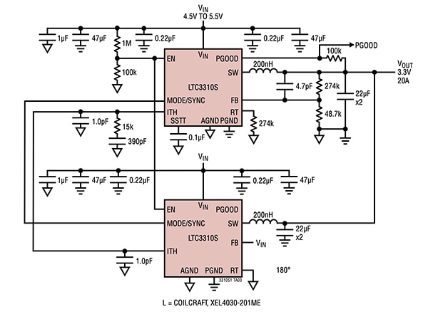 Figure 8: With a few additional components, two or more LTC3310 devices can be combined for multiphase higher current operation; shown is the two-phase/20 A configuration. (Image source: Analog Devices)
Evaluation boards shorten design cycles
Regulators such as the LTC3310 devices are direct in their application as they have no initialization registers, software-controlled functions, or other setup complexities. Nonetheless, it makes technical sense to be able to assess their static and dynamic performance and optimize passive-component values before committing to a final layout or BOM specifics. The availability of LTC3310 evaluation boards make this process much easier. Analog Devices offers a selection of such boards matched to different LTC3310 versions and configurations:
- The DC3042A supports the adjustable output LTC3310 device (Figure 9).
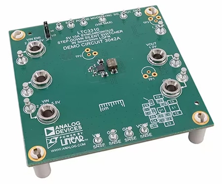 Figure 9: The DC3042A evaluation board is designed for the LTC3310 with a user-settable output voltage. (Image source: Analog Devices)
In addition to instructing users on basic setup and operation, the documentation includes a schematic diagram, board layout, and bill of materials (BOM). It also calls out the various test points and connections, as well as the probing arrangement for measuring output ripple and step response (Figure 10).
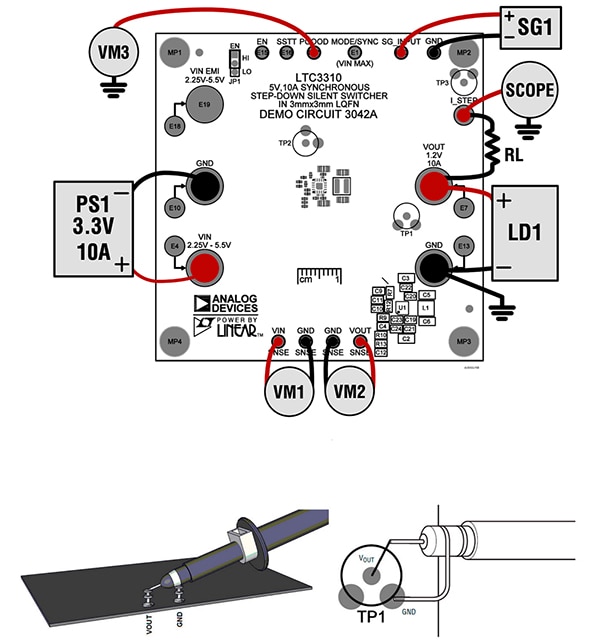 Figure 10: The DC3042A user demo manual clearly calls out test points and connections (top), as well as the probing setup and configuration for measuring output ripple and step response. (Image source: Analog Devices)
- For the LTC3310S-1 with a fixed output voltage, there’s the DC3021A evaluation board (Figure 11).
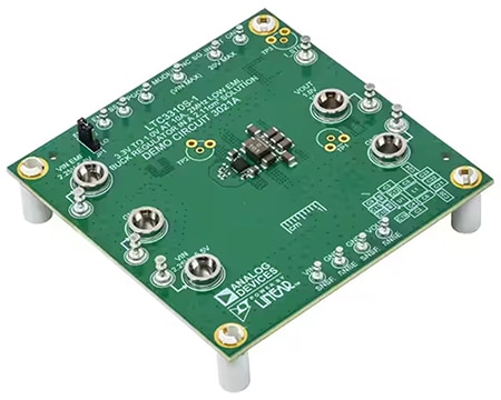 Figure 11: For the LTC3310S-1 with an output voltage that is not user adjustable, the DC3021A evaluation board is the appropriate choice. (Image source: Analog Devices)
- Finally, for the somewhat more-complex multiphase paralleled arrangement, there’s the DC2874A-C (Figure 12). This evaluation board has the LTC3310S operating as a multiphase 2.0 MHz, 3.3-to-1.2-volt buck regulator. The DC2874A has three build options to provide two-phase/20 A, three-phase/30 A, or four-phase/40 A output solutions.
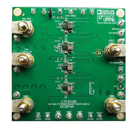 Figure 12: The DC2874A-C evaluation board for the LTC3310S has three build options: two-phase/20 A, three-phase/30 A, or four-phase/40 A outputs. (Image source: Analog Devices)
By using the LTC3310S and investing some time with the appropriate evaluation board and its corresponding user manual, designers can minimize the time spent on DC/DC regulator performance.
Conclusion
Engineers have traditionally had to choose between two conflicting DC/DC regulator topologies with distinctly opposing attributes. LDOs offer very low-noise DC output but with low-to-moderate efficiency, making them a thermal challenge beyond outputs of about 1 A. In contrast, switching regulators offer efficiencies in the 90% range, but add noise to the DC output rail, and are also a source of conducted—and especially radiated—noise that can easily result in the product not passing mandatory regulatory tests.
Fortunately, the Silent Switcher families from Analog Devices employ a variety of innovative design techniques that overcome this “choose one or the other” dilemma, resulting in highly efficient, very-low-noise, tiny form-factor regulator options.

Disclaimer: The opinions, beliefs, and viewpoints expressed by the various authors and/or forum participants on this website do not necessarily reflect the opinions, beliefs, and viewpoints of DigiKey or official policies of DigiKey.


