How SCARA, Six-Axis, and Cartesian Pick-And-Place Robotics Optimize and Streamline Electronics Manufacturing Processes
Contributed By DigiKey's North American Editors
2023-07-12
Introduction
By some estimates, the use of robotics in electronics manufacturing now rivals that of the automotive industry. No wonder: Fabricated chips, components, and fully assembled electronics are high value, so they justify investments in automation technologies. Complicating matters is that volumes and therefore throughput must be high, and the products are also inherently delicate … with semiconductor wafers for some applications now only 140 µm thick. These application parameters demand precision handling with motion systems and robotics having exceptional reach, speed, force, and dexterity as well as cleanroom compliance.
 Figure 1: Here, a delicate wafer is placed into an atomic layer deposition machine located within a cleanroom. (Image source: Dreamstime)
Hastening the adoption of robotics in semiconductor manufacture are burgeoning classes of six-axis robots, selective compliance assembly robot arms (SCARAs), cartesian machinery, and collaborative robots featuring reconfigurable or modular hardware as well as unifying software to greatly simplify implementation.
These robots and their supplemental equipment must be designed, rated, and installed for cleanroom settings or else risk contaminating delicate wafers with impurities. Requirements are defined by ISO 14644-1:2015, which classifies cleanroom air cleanliness by particle concentration. So, there’s especially heavy reliance on:
- Exacting integration, wrapping, delivery, and installation methods to prevent particulate from hitchhiking into the cleanroom
- Specialty coatings that won’t flake or otherwise degrade
- Stainless steel enclosures and other elements wherever feasible
- Specialty inert and non-gassing lubricants for mechanical components
- Vacuum elements within the robotic body to direct any particulate to a segregated exhaust area
- Specialty sealing of all robot joints
The latter is especially important for high-speed robots that satisfy the need for high semiconductor throughput but shed more particles than slower-moving equipment.
 Figure 2: The use of robotics and other automation for the production of micro-electronics extends beyond the cleanroom. (Image source: Dreamstime)
Summary of where each robotic type excels
Though application overlaps abound, six-axis robots are most strongly associated with electronic device assembly. SCARAs maneuver electronic components through 360° to execute pick-and-place wafer handling and processing tasks faster and often more precisely than other options. Cartesian robots in contrast are often associated with semiconductor testing and packaging tasks as well as the processing of large-format electronic products. On the other hand, collaborative robots (cobots) are used to bridge highly protected cleanroom zones to sections of cleanrooms that can be traversed by plant personnel. Cobots are also seeing increased use in soldering and other tasks once the near-exclusive domain of manual operations.
 Figure 3: Shown here is the automated soldering of chip components onto a PCB. (Image source: Dreamstime)
Though beyond the scope of this article, the parallel-kinematics design known as delta robots is also seeing increased adoption — especially for electronic products assembly. Whether operating alone, ganged in pairs, or installed to complement SCARAs in a workcell, delta robots in semiconductor manufacture provide exceptionally quick and dynamic picking and packing capabilities. Read more about these applications in the digikey.com How Delta Robotics Optimize and Streamline Electronics Manufacturing Processes article on delta robots in the semiconductor industry. In fact, the kinematics of deltas impart accuracy and repeatability for suitability in the assembly of photovoltaic electronics.
Robotics rely on end effectors for productivity
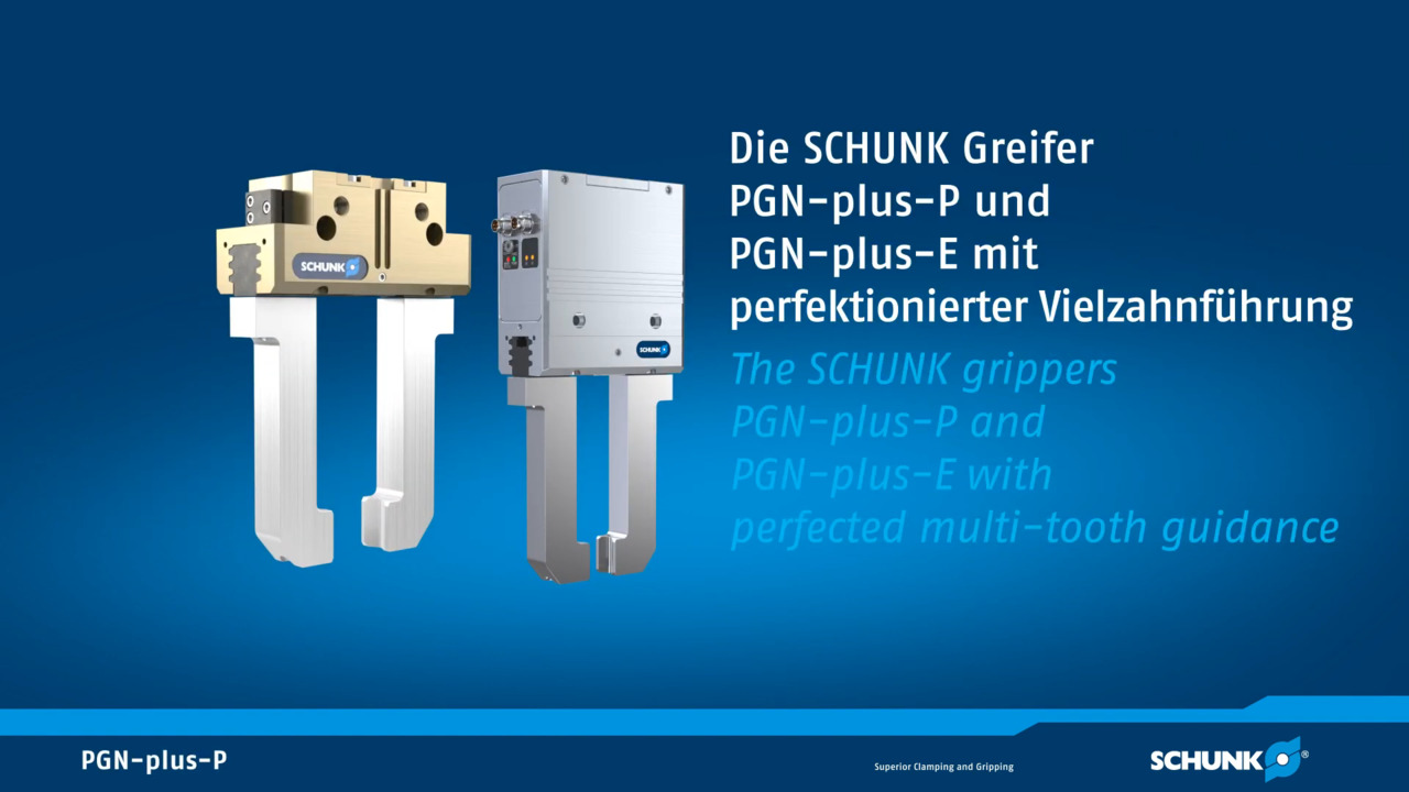
Advanced cleanroom-rated robotic end-of-arm tooling (EoAT or end effectors) such as grippers are core to semiconductor production. Here, EOATs must have high dynamics and the ability to execute tracing, placing, and assembling with exacting precision. In some cases, EoAT force feedback or machine vision boosts parts-handling accuracy by imparting adaptive capabilities — so pick-and-place routines are quickly executed even if there’s some variability in workpiece positions, for example. Such sensor and feedback advancements can sometimes render the complicated electronics-handling fixtures of legacy solutions unnecessary.
 Figure 4: Small-component EGK grippers are lubricated with H1 grease and sport cleanroom certification. (Image source: SCHUNK Intec Inc.)
 Figure 5: Electronics contract manufacturing makes copious use of robotics for board testing. (Image source: Dreamstime)
Consider how flexible workcells served by six-axis robots often execute two or more tasks such as general workpiece handling, conveyor and other machine tending, machining, assembly, and packaging. Similarly, the application of encapsulation, vibration damping, shielding, adhesion, and sealing materials is often executed within one six-axis robotic workcell. Here, robotic end effectors complemented by automated tool changers impart multitasking capabilities so every workcell is maximally useful; EoAT changeovers are typically fast to support the semiconductor industry’s high throughput requirements. For example, a robot might employ one EoAT to pick and place items into a fixture. Then (after a quick EoAT changeover) it might apply adhesive and press together mating housing halves of an end product. A third EoAT might load finished items onto an outbound conveyor or into a case.
 Figure 6: Robotic end effectors can take the form of soldering iron tips to automate the assembly of subcomponents onto PCBs. (Image source: Dreamstime)
SCARA robotics in electronics manufacturing
For decades, SCARAs have remained the gold standard for semiconductor wafer processing, handling, and assembly tasks including:
- Deposition and etching
- Thermal processing
- Reticle processing
- Circuit board assembly
- Testing and metrology
After all, SCARAs offer high speeds throughout their cylindrically shaped 360° reach — often capable of executing pick-and-place tasks far faster (and sometimes more precisely) than comparable six-axis and cartesian solutions. More specifically, some industry-typical SCARAs deliver repeatability to within ±20 μm on linear degrees of freedom (DOFs) and ±0.01° on the angular axis — as well as direct-drive options for smooth transport of thin and relatively brittle wafers. While payloads can be limited to 10 kg or lighter for many SCARAs, that’s rarely an issue in semiconductor applications — though is certainly a consideration for the related field of solar-panel production.
 Figure 7: SCARA robots execute pick-and-place wafer handling and processing tasks quickly and precisely. (Image source: Dreamstime)
SCARAs pair well with conveyors used in semiconductor processing stations as well as wafer carousels (also called rotary tables) designed to facilitate the addition of components or features to multiple circuit boards at a time.
Six-axis robotics in electronics manufacturing
Industrial-grade articulated robots feature multiple rotary joints to manipulate objects through two to 10 DOFs. The most common articulated-robot format is the six-axis robot. Semiconductor processes necessitating cleanroom settings benefit from six-axis robots that are suitably rated as well as compact to consume less power and less of the premium cleanroom real estate. Variations abound to deliver the speed and accuracy needed for high-throughput handling and assembly. The servomotors to drive the robots’ joints are similar to those found in other robot types, but six-axis robots are far more likely to pair these motors with strain-wave or cycloidal gearing.
Like SCARAs, six-axis robots also pair well with conveyors used in semiconductor processing stations.
 Figure 8: This six-axis articulated robot is available in ISO 5 (class 100) cleanroom models. (Image source: Denso Robotics)
The main strength of six-axis robots is their dexterity and large working volume for a given linkage-set size — whether installed on a floor base or inverted from a ceiling. To illustrate, a six-axis arm that’s 600 mm tall when folded might reach 650 mm in all directions with the ability to quickly and concurrently sweep each joint 120° to 360° for nimble movement of electronic payloads of a few grams to several kilograms or more. Absolute encoders at each joint and Ethernet-based networking provide motion feedback and connectivity for PLC, PC, or dedicated robot controls and adaptive software to both command and improve processes over time. These controls include the integration of sophisticated end effectors — for example, grippers to safely handle small and fragile electronics components.
Six-axis robots excel at machine tending and the packaging of electronics products. Beyond the assembly of the boards themselves, the robots can fasten electronics into end products’ metal or plastic housings and make the necessary electrical connections as well. Some six-axis robots can also execute finished electronics products kitting, case packing, and palletizing.
Cartesian robotics in electronics manufacturing
Cartesian robots — those based on modular stacks of linear axes — help operations satisfy the semiconductor industry’s need to maintain cleanroom conditions for many processes. Nearly unlimited scalability means travel can cover anything from a few centimeters to more than 30 meters. Cartesian robot repeatability can stay within ±10 μm on linear DOFs with comparable angular repeatability from end effectors as well as rotary-to-linear and direct-drive options for especially smooth transport of wafers. Speeds to six meters per second are common.
 Figure 9: Cartesian robots execute fully automated semiconductor manufacturing tasks. Note the linear motors that provide high-precision direct driving on the critical axis. (Image source: Dreamstime)
Cartesian machinery typically executes dedicated automation tasks, as its kinematics tend to be less flexible and reconfigurable than that of other robotic types. However, accuracy is exceptional … especially when controls use feedback and generate commands for millisecond responsiveness. Such motion is key for automated board manufacturing; trimming and surface polishing; and extensive assembly routines.
Cartesian robotics stations are also the top choice for large-format electronics such as flat-panel displays and solar panels.
Specific cartesian robotics application example
Consider cartesian robotics in maximally automated printed circuit board (PCB) manufacture and assembly. Cartesian robotics either maneuver end effectors over the boards or take the form of cartesian tables that move PCBs through the reach of fixed processing equipment. For example, such tables might move boards through lithography equipment to print copper circuits onto a nonconductive silicon substrate. Then after the initial PCB print process, copper not part of the design circuitry is chemically etched off. Nonconductive solder masks isolate adjacent traces and components.
 Figure 10: Cartesian robotics can be fitted with imaging equipment (such as this thermal-imaging camera) for thermography of PCBs produced with laser-assisted bonding techniques. (Image source: Teledyne FLIR)
In many PCB assembly operations, cartesian robotics accept electronic subcomponents on reel tapes or box tapes fed into the workcell. (The robotics’ pick-and-place head is designed to grasp and place a variety of these subcomponents.) The robotics verify each subcomponent value and polarity and then set and solder the subcomponents via through-hole or surface-mount technology (SMT) attachments. Through-hole subcomponent leads insert into board holes, get trimmed and clinched, and then get soldered to the board backside for top mechanical strength (though necessitating more complicated assembly routines). In contrast, SMT subcomponents accept maximally automated high-volume set and solder routines … so they now dominate many board designs. That said, through-hole mounting is still most common for attaching large capacitors, transformers, and connectors to boards.
 subcomponents to a board")
 subcomponents to a board") Figures 11a and 11b: Shown here are tool heads for affixing surface-mount technology (SMT) subcomponents to a board. (Image source: Dreamstime)
Figures 11a and 11b: Shown here are tool heads for affixing surface-mount technology (SMT) subcomponents to a board. (Image source: Dreamstime)
For SMT components, solder paste is pre-applied to the PCB before component assembly. Reflow soldering then uses hot air to melt the solder paste to form the SMT component connections. Wave soldering is more common for through-hole components; this involves passing the board across a standing wave formed on the surface of a pan of molten solder. Such machines are costly and best suited to very high-volume manufacturing.
 Figure 12: Machine-vision feedback often informs cartesian system responses. Massive onboard processing power, advanced algorithms, and an FPGA let HAWK smart cameras (including the model shown here) achieve real-time trigger response for code reading, verification, inspection, and guidance for 4,000 to 14,000 parts per minute. In fact, this camera is an intermediate solution between complex PC-based cameras and basic industrial smart cameras. (Image source: Omron Automation and Safety)
Typical motors and drives for cartesian robotics
Cartesian robotics use many of the same types of servomotors, precision gearing, and electromechanical drives as other robotics solutions. One caveat is that the stepper motors in some cartesian designs that transport semiconductors during production shouldn’t be confused with so-called step-and-repeat cameras — sometimes simply called steppers. The latter are essential to photolithography processes during chipmaking.
Just as SCARA and especially six-axis robotics have made increased use of direct-drive torque motors, cartesian robotics have (in designs to serve the semiconductor industry) made increased use of linear motors in recent years. A variety of industry-standard and proprietary motor coils, miniature end positioners, piezo-based adjustment modules, vacuum and cleanroom-rated subsystems, linear bearings, controls, and other innovations complement these direct drives to help cartesian systems output ultra-fine ultra-fast motions.
Collaborative robotics in electronics manufacturing
Collaborative robots (cobots) have proliferated in the semiconductor industry over the last decade. For more reasons about this, see the DigiKey.com blog, Easy Automation with Omron TM Collaborative Robots. In semiconductor manufacture, cobots from Omron and other makers can prevent the extremely costly contamination of wafers by bridging protect wafer workzones and those serviced by cleanroom personnel. Semiconductor-production grade cobot installations also prevent particulate and lubricant outgassing contamination while complementing manual operations for placing and soldering.
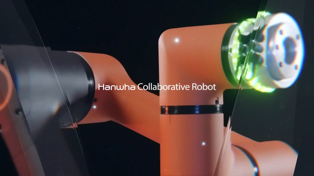
 Figure 13: Cobots in the HCR-5 series meet ISO-2 cleanroom specifications. (Image source: Hanwha Corp./Momentum)
") Figure 14: KUKA collaborative robots (cobots) are core to the design of this Infineon ISO3 wafer-processing cleanroom. (Image source: KUKA)
Figure 14: KUKA collaborative robots (cobots) are core to the design of this Infineon ISO3 wafer-processing cleanroom. (Image source: KUKA)
 Figure 15: KUKA cobots in this Infineon cleanroom were expertly integrated, networked, and programmed by mechatronic and automation specialists. (Image source: KUKA)
Cobots in the semiconductor and electronics industry must have above-average speed capabilities complemented by advanced dynamics and controls to prevent the jarring of thin and therefore delicate wafers. Otherwise, tiny cracks can form. Of course, breakage is far less likely with properly specified cobots than human labor.
Automated soldering with cobots is also appropriate where components are being assembled onto especially thin boards and the effects of silicon thermal expansion are a concern. Where cobots are destined to perform this and other assembly tasks, it’s often logical to integrate thermography or other board-inspection equipment onto the EoAT. That speeds error-proofing tasks for higher yields and quality assurance … often at relatively low cost.
Conclusion
Industrial robotics can provide affordable and flexible automation of semiconductor and electronics production. Technical challenges are the need to satisfy cleanroom ratings, high throughput, and careful handling of exceedingly expensive workpieces. Even so, today’s robotic hardware as well as robotic simulation software and programming have simplified the sizing and selection of cleanroom robotic solutions.
Complicating matters is how increasingly fine details on increasingly miniaturized electronics necessitate roboticized assembly processes that follow suit. Robotics have risen to this challenge with motors, mechanical linkages, controls, and networks that allow evermore advanced capabilities. Complementary technologies such as machine vision and real-time industrial networking have also imparted new capabilities in robotics for manipulating, processing, and assembling high-volume semiconductor production.
Disclaimer: The opinions, beliefs, and viewpoints expressed by the various authors and/or forum participants on this website do not necessarily reflect the opinions, beliefs, and viewpoints of DigiKey or official policies of DigiKey.