Balancing MCU Performance and Power Consumption with Integrated Features
Contributed By DigiKey's North American Editors
2017-05-10
Developers have had access for some time to MCUs that feature low-power operating states, shutting down peripherals and even the core itself to reduce system power requirements. For some applications, however, developers need more direct control over power utilization to ensure that portions of the system remain powered to meet key functional requirements.
Designers have in the past used standalone power management devices to build in precise power control. In contrast, the Analog Devices ADuCM3029 MCU offers an integrated solution that can help developers more easily achieve maximum performance while minimizing power consumption in designs built for sensor data acquisition, wearables, and other Internet of Things (IoT) applications.
MCU’s addressing power management
For low-power designs, engineers can find a wide range of advanced MCUs designed with power saving options. Devices targeting power sensitive applications routinely feature capabilities such as frequency scaling that allow engineers to trade performance for reduced power.
Typically, low-power modes offer graduated power reduction by shutting down more and more MCU subsystems until only the minimal circuitry required to wake the MCU remains operational. As a further refinement for power management, ultra-low-power MCUs add special operating modes that separately manage power to the device’s core and its peripherals. Even in these cases, these special modes sometimes shut down peripherals as a group, or use automated mechanisms that grant the developer little control over the details of power allocation.
Although MCU power management typically provides a range of low-power operating modes, the transition to a lower-power mode typically brings a steep drop in functionality. In many cases, applications can tolerate loss of functionality for limited periods. In some cases, however, precise control of power consumption is essential for maintaining operation. The Analog Devices ADuCM3029 processor is designed specifically to support more complex power management requirements in ultra-low-power applications.
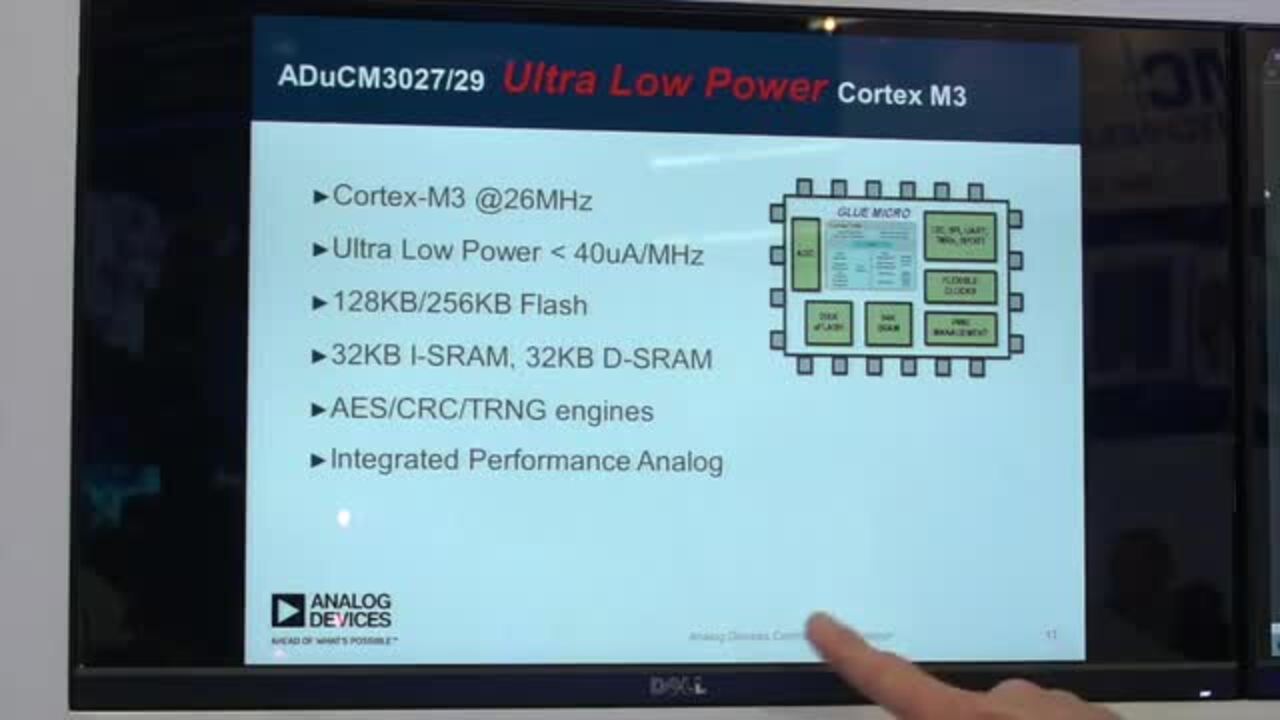
Built around an ARM® Cortex®-M3 core, the ADuCM3029 offers 256 Kbytes of error correcting code (ECC) flash and 64 Kbytes of configurable SRAM with multi-parity bit protection. A variant, the ADuCM3027, has 128 Kbytes of flash, but otherwise provides the same features and functionality as the ADuCM3029.
Along with an integrated hardware crypto accelerator, the devices include an 8-channel, 12-bit analog-to-digital converter (ADC), as well as multiple digital peripherals including SPI, I2C, UART, GPIOs, synchronous serial port (SPORT), and 25-channel DMA controller. Even with its extensive functionality, the device typically consumes less than 30 μA/MHz in active mode. With the ADuCM3029, however, designers can further tune the balance between functional performance and power consumption.
Tuning power/performance
As with most advanced MCUs, the ADuCM3029 features multiple power modes designed to reduce power during periods of low activity. In hibernate mode, the device typically consumes less than 750 nA by turning off the processor core and most peripherals, while maintaining power to program-selected SRAM regions. For periods when the application is inactive, the device’s shutdown mode requires only 60 nA.
However, developers frequently face scenarios that require some degree of peripheral activity when the processor is inactive. To address this issue, the ADuCM3029 provides an additional power mode called flexible sleep (Flexi) mode. Flexi mode brings power consumption down to as little as 300 μA, while providing functionality that lies between active and hibernate modes. In Flexi mode, the device core remains in sleep mode while specific peripherals specified by the developer remain active (Table 1).

Table 1: The Analog Devices ADuCM3029 MCU’s power modes automatically enable (green) or disable (red) power to certain on-chip blocks, but still allow developers to control power to certain peripherals (orange) or even configure the size of SRAM retained (*) during hibernate mode. (Table source: Analog Devices)
Developers can place the MCU in Flexi mode simply by setting the MODE bits in the device’s PMG_PWRMOD register to 0 and executing the WFI (wait for interrupt) instruction. With the processor core inactive, the developer can keep specific peripherals functional by writing 0 to each peripheral’s corresponding bit in the MCU’s CLKG_CLK_CTL5 register. Although the device cannot execute instructions in this mode, it can continue to perform activities such as DMA transfers between peripherals to memory.
Providing the ability to maintain peripheral operations, Flexi mode offers a power efficient solution to a common problem in sensor applications where one or more sensors need to be sampled over a period of time before involving the processor. In this case, developers can use the integrated ADC’s auto-cycle mode to perform one or multiple conversions on selected channels, and set the DMA controller to transfer the samples automatically to SRAM. After a programmer-specified number of conversions and the associated DMA transfer, the DMA controller issues an interrupt to wake the core for subsequent processing of the sampled data (Figure 1).

Figure 1: In Flexi mode, the Analog Device ADuCM3029’s core processor sleeps while select peripherals continue to operate, allowing operations such as DMA transfer of multiple channels of ADC samples that wake the processor only upon completion. (Image source: Analog Devices)
Cache and clocks
In trading functionality for performance, Flexi mode and the other low-power modes offer designers a powerful mechanism for significantly reducing power in their designs. For many applications such as battery-powered systems, however, designers often need finer control over power consumption. With the ADuCM3029, designers can further reduce power by taking advantage of a combination of conventional and novel methods.
Among typical conventional methods, the use of instruction cache can reduce access to off-chip memory or power hungry on-chip memory such as Flash. In ADuCM3029-based systems, developers can allocate as much as 4 KB of SRAM to serve as cache. In practice, specific power savings depends on cache hit rates, but Analog Devices notes that the use of cache in some typical benchmark applications can significantly reduce power consumption (Table 2).
|
Table 2: Configuring the Analog Device ADuCM3029 to use some of its SRAM as cache, typical benchmark applications can run at power levels approaching low-power SRAM access rather than higher power flash access. (Table source: Analog Devices)
Frequency scaling is another long-standing approach for reducing power. Lower processor clock rates slow execution instruction but also result in lower power consumption (Figure 2). Unlike many other approaches, however, the ADuCM3029 lets developers dynamically modify clock frequencies separately for the processor and for the peripherals. Here, the device uses a phase-locked loop and clock dividers driven by a 26 MHz internal oscillator or external crystal to generate clocks for on-chip resources including the processor, memory, and interfaces. A 32 kHz internal oscillator or external crystal drives the device’s real-time clocks (RTCs) and watchdog timer. Developers can modify the device’s respective clock registers during runtime to change clock frequencies to match changing application requirements or opportunities for power reduction.

Figure 2: Designers simply set a few registers in the Analog Device ADuCM3029 to scale the MCU’s clock frequency on the fly and achieve a corresponding drop in power consumption. (Image source: Analog Devices)
Enhanced power path
Along with its support for more conventional power reduction methods, the ADuCM3029 offers more novel approaches based on specialized device hardware features. Designed into the ADuCM3029’s power path, an on-chip buck converter bridges the difference between the device’s supply voltage range, VBAT (1.74 V - 3.6 V), and the internal digital domain operating voltage (1.2 V).
In normal operation, an integrated low-drop-out (LDO) regulator sources this internal voltage. As with any typical LDO, when the difference between the LDO’s supply and load voltage is high, the default power path simply dissipates excess energy, resulting in wasted power. With this MCU, however, designers can reduce this loss at higher supply voltages with only a few external capacitors (Figure 3). On the software side, developers simply write to the buck control register (PMG_CTL1) to enable the buck converter.

Figure 3: Using just a few lines of code and some external capacitors, developers can enable the Analog Device ADuCM3029’s on-chip buck converter to reduce the voltage level applied to the device’s LDO regulator. (Image source: Analog Devices)
Based on a high-efficiency, capacitor-based charge pump topology, the converter reduces the voltage level supplied to the LDO. Consequently, the MCU exhibits a dramatic reduction in power consumption at voltage levels on the high end of VBAT (Figure 4). At levels below about 2.3 V, the buck converter enters bypass mode and follows VBAT.
 voltage levels above about 3 V")
Figure 4: At supply (VBAT) voltage levels above about 3 V, the ADuCM3029’s on-chip buck converter reduces MCU power consumption, achieving a 50% relative reduction in active mode, shown here, as well as in Flexi mode. (Image source: Analog Devices)
Power-optimized sampling
Features like caching, frequency scaling, and on-chip DC-DC conversion work at the system level to help reduce power consumption. At the application level, features like Flexi mode aid in power reduction for peripheral operations such as sensor sampling. Yet, even these methods can prove insufficient in some applications. For example, battery-powered IoT devices are often tasked with sampling sensors at very low acquisition rates, or periodically monitoring some external process.
For applications with slow periodic activity, developers typically rely on the MCU’s RTC to maintain a consistent time base, as well as drive countdown timers used to wake the MCU at precise, predetermined times. Consequently, advanced MCUs typically feature power modes that retain RTC functionality even in very low power modes. With the ADuCM3029, developers have access to two separate RTCs, RTC0 and RTC1, that provide additional options for balancing power and performance.
As noted in Table 1, both RTCs support operation in active, Flexi, and hibernate modes, but only RTC0 remains available during the lowest power shutdown mode. Within the other modes, however, distinct differences between the two clocks provide developers with flexibility in implementing more complex timing applications. For example, RTC0 counts time at 1 Hz in units of seconds, limiting it to wake up times specified only in seconds. RTC1 can be prescaled across a wide range and provide wake up times down to 30.7 μs. Power for each clock differs as well. RTC0 is powered from the primary supply (VBAT), while RTC1 is powered by the internal 1.2 V power domain. As such, use of the optional buck converter further reduces RTC1’s effective power consumption. Perhaps more importantly, RTC1 supports Analog Device’s SensorStrobe mechanism, a unique low-power sampling feature built into the ADuCM3029.
SensorStrobe is a special RTC1 alarm that generates an output pulse on the MCU’s RTC1_SS1 pin. Developers can connect the ADuCM3029’s SensorStrobe output to an external multi-sensor device such as the Analog Devices ADXL363 to create a very low-power sampling solution with only a few components (Figure 5).

Figure 5: The ADuCM3029’s SensorStrobe mechanism provides a stable, synchronized alarm to external devices, allowing implementation of a simple data-acquisition system when combined with an integrated sensor such as the Analog Devices ADXL363. (Image source: Analog Devices)
Analog Devices provides the specific subsystem shown in Figure 5 as part of its ADuCM3029 EZ-KIT development kit, the ADZS-UCM3029EZLITE. Along with a simple hardware configuration, this approach requires only a few lines of code to set up the associated device registers and start the SensorStrobe mechanism (Listing 1).
#define PRD_VAL 255
void SensorStrobe_Cfg()
{
// SensorStrobe Pin Mux
*pREG_GPIO2_CFG |= (0x3 << BITP_GPIO_CFG_PIN11);
// Reset the RTC counter
while(*pREG_RTC1_SR1 & 0x0180); //wait until sync
*pREG_RTC1_SR0 = 0xFF;
*pREG_RTC1_CR0 = 0;
while(!(*pREG_RTC1_SR0 & 0x0080 )); //wait for sync
// SensorStrobe configuration
// Initial trigger and auto reload value = 255 RTC counts
// RTC runs at 32KHz ideally, 1 RTC count = 30.7us
while(*pREG_RTC1_SR5 != 0);
*pREG_RTC1_SS1ARL = PRD_VAL;
// SensorStrobe to be triggered after 255 RTC counts
*pREG_RTC1_CR4SS = (1 << 9); //Enable Autoreload
*pREG_RTC1_SS1 = PRD_VAL; // Initial Compare Value
// Enable SensorStrobe
*pREG_RTC1_CR3SS = 1;
while(*pREG_RTC1_SR4 != 0x77FF);
// Initialize the counter value to zero
while(*pREG_RTC1_SR1 & 0x0600);
*pREG_RTC1_CNT0 = 0;
*pREG_RTC1_CNT1 = 0;
while(!(*pREG_RTC1_SR0 & 0x0400));
// Enable (start) the counter
while(*pREG_RTC1_SR1 & 0x0180); //wait until sync
*pREG_RTC1_SR0 = 0xFF;
*pREG_RTC1_CR0 = 1;
while(!(*pREG_RTC1_SR0 & 0x0080)); //wait for sync
return;
}
Listing 1: Developers need set only a few device registers to take advantage of the Analog Devices ADuCM3029 MCU’s SensorStrobe feature. (Image source: Analog Devices)
During SensorStrobe operation, developers place the ADuCM3029 in hibernate mode to ensure minimum MCU power consumption during the extended sampling process. While the MCU remains in hibernate mode, RTC1 counts to the desired value specified in register values established during SensorStrobe setup. When the SensorStrobe count conditions are met, the SensorStrobe signal is applied to the ADXL363’s interrupt input pin, waking that device. In turn, the ADXL363 runs its own data sampling routines. On completion, the ADXL363 issues a signal on the MCU’s interrupt pin, causing the MCU to wake from hibernate mode and begin processing the sampled data.
In the past, developers routinely implemented this kind of extended sampling design using an external RTC, timer, or even a simple oscillator. Besides adding to design complexity, use of an external clock source breaks time synchronization between the sampled data and the MCU’s own time base. As such, developers using the earlier approach have needed to effectively resample their data to normalize its timestamp to that of the MCU. By using RTC1 in SensorStrobe mode, however, developers can ensure that sample timestamps remain synchronized to the ADuCM3029 based system itself.
Developers can potentially find a number of discrete mechanisms that approach the integrated power management capabilities of the ADuCM3029. However, by leveraging that device’s internal capabilities, engineers can easily achieve a better match between power and performance.
Conclusion
Demand for lower power systems continues to challenge developers’ ability to achieve maximum performance in smaller, power efficient designs. Compounding their difficulty, each application requires a unique balance between functional performance and power consumption.
The integrated power management features of the Analog Devices ADuCM3029 MCU provides developers with the flexibility required to more easily find that balance. Using this device, developers can deliver the unique combination of high performance and low power required for each specific application.
Disclaimer: The opinions, beliefs, and viewpoints expressed by the various authors and/or forum participants on this website do not necessarily reflect the opinions, beliefs, and viewpoints of DigiKey or official policies of DigiKey.