Analog Fundamentals: How Sample and Hold Circuits Work and Ensure ADC Accuracy
Contributed By DigiKey's North American Editors
2020-04-22
Converting an analog signal from the “real” world to a digital signal that can be processed upstream is a fundamental function of electronic systems, ranging from audio recording to the Internet of Things (IoT), the Industrial IoT (IIoT), and now the artificial intelligence (AI) of Things (AIoT). However, to perform it effectively and efficiently requires a level of understanding of the underlying principles and steps that are often overlooked.
For instance, how exactly is a signal “held” and then “sampled” before conversion, given that a typical analog signal applied to the input of an analog-to-digital converter (ADC) is changing amplitude continuously and will be different at the end of the conversion than it was at the beginning? This amplitude change or skewing can result in a serious error, especially for high resolution ADCs which take more time to convert a signal. The challenge for designers is to both understand and eliminate this source of error.
This article shows how preventing amplitude skew is accomplished using a sample and hold (S&H) or track and hold (T&H) circuit for the ADC. The S&H (or T&H) performs the true sampling of the input and operates between the input anti-aliasing low-pass filter and the ADC. The article discusses the characteristics and selection criteria for S&H ICs and looks at ADCs with integrated S&Hs. Example devices with varying characteristics for different applications from Texas Instruments, Maxim Integrated, and Analog Devices are used for illustrative purposes.
The role of sample-and-hold in ADCs
When a non-DC signal is applied to the input of an ADC, it is changing amplitude continuously. However, the analog-to-digital conversion process takes a finite interval of time, so over that time, the amplitude of the ADC input will change (Figure 1). It is this amplitude skewing that results in a potentially serious error.
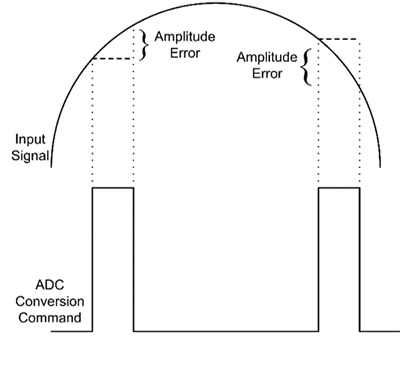 Figure 1: An ADC with a varying input signal is subject to amplitude errors (top) due to the signal amplitude variations during digitization (bottom). (Image source: DigiKey)
Preventing amplitude skew in an ADC is a matter of sampling the signal and holding a fixed amplitude while the conversion is in process. This is accomplished using the S&H or T&H circuit for the ADC (Figure 2).
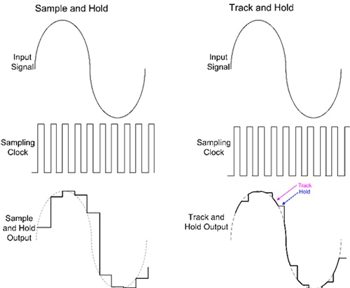 Figure 2: The primary difference between an S&H (left) and a T&H (right) circuit is the duration of the tracking period: it is short in the S&H and long in the T&H. (Image source: DigiKey)
Both types of circuits sample the input signal and hold the sampled voltage constant for the duration of the conversion process. The T&H circuit output (right) tracks the input signal until signaled to sample; it then holds the sample value during the ADC conversion. The S&H has a shorter sample aperture and its output is a series of sampled levels (left). The key difference between T&H and S&H is the duration of the tracking interval: very short for the S&H and significantly longer for the T&H. Both circuits rely on a fast switch to isolate a storage capacitor that has been connected to the signal input. The balance of this article will use S&H synonymously with S&H or T&H.
The S&H stage performs the true sampling of the input and operates between the input anti-aliasing low-pass filter and the ADC. The low-pass filter performs anti-aliasing band limiting and must precede the S&H to bandlimit the signal before sampling to prevent aliasing (Figure 3).
 Figure 3: In the digitizer signal path, the S&H is placed between the anti-aliasing low-pass filter and the ADC. (Image source: DigiKey)
Note that the signals before the S&H are all analog signals. The output of the S&H is a sampled waveform that is fed to the ADC.
A typical S&H device
The block diagram of the Texas Instruments LF398MX/NOPB S&H integrated circuit (IC) shows the basic circuit configuration (Figure 4). The S&H is implemented using a fast switch and a high quality capacitor. In the case of the LF398MX/NOPB, the capacitor is external to the IC. When the switch is closed, the capacitor is charged to the input signal voltage level. When the switch is open, the capacitor retains that voltage until it is digitized by the ADC. This S&H uses bi-FET technology, which combines FETs with bipolar transistors, to support fast acquisition (less than 6 microseconds (µs) with 0.01% amplitude error) with high DC accuracy (typically 0.002%), and an extremely low voltage droop (typically less than 83 microvolts (µV) per second). Internal amplifiers buffer the switch and hold capacitor.
The acquisition time of the S&H is dependent on the value of the hold capacitor, which can be in the range of 0.001 to 0.1 microfarad (µF). The external hold capacitor has to have low dielectric absorption and low leakage. Polystyrene, polypropylene, and teflon capacitors are recommended.
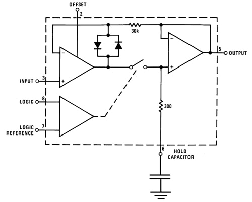 Figure 4: The block diagram of the Texas Instruments LF398MX/NOPB S&H shows the key components: a fast switch and an external hold capacitor. (Image source: Texas Instruments)
S&H characteristics
S&H devices have a number of specific terms to describe their operation (Figure 5).
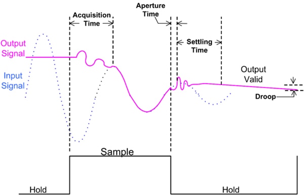 Figure 5: The definitions of common S&H dynamic characteristics include acquisition time, settling time, aperture time, and amplitude droop. (Image source: DigiKey)
Acquisition time is the time from switching into sample mode until the S&H begins tracking the input signal. It is a function of the value of the hold capacitor and the series resistance of the switch and the signal path. When the mode returns to hold, there may be a time delay until the device stops tracking the input and begins to hold a value—this is the aperture time. Aperture time is a function of propagation delays of the drivers and the switch. Aperture uncertainty or jitter is the variation in the aperture time due to clock variations and noise.
Once in the hold mode, there is a time between entering that mode and when the device settles to within an error band about the hold value called the settling or hold settling time. Part of the settling time may include an unwanted transfer of charge between the switch driver and the hold capacitor; this is called the hold step or pedestal error. Hold step usually has magnitudes in the millivolt (mV) range and its effect is minimized by keeping the full-scale range of the signals as high as possible.
The shortest sampling period for the S&H is the sum of the acquisition time, aperture time, and the settling time. The maximum sampling rate possible is the reciprocal of the sum of the acquisition time, aperture time, and settling time.
While in the hold mode, the S&H hold value may decrease due to leakage from the hold capacitor. This voltage increment is called droop. It is usually specified as a droop rate in mV per second.
S&H configurations
S&H ICs are available in many configurations to match application needs. Consider an application requiring differential inputs such as interfacing with a differential output transducer like an accelerometer, strain gage, or optical current monitor. The Maxim Integrated DS1843D+TRL is a good example of an S&H IC for such applications (Figure 6).
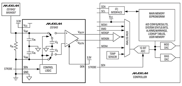 Figure 6: As shown in this typical operating circuit, the Maxim Integrated DS1843+TRL is a differential S&H that uses dual hold capacitors to implement differential sampling. (Image source: Maxim Integrated)
The DS1843+TRL shown is in a typical optical line transmission application for burst mode received signal strength indicator (RSSI) measurement. The Maxim Integrated DS1842/MAX4007 is a current monitor that mirrors a current from an avalanche photodiode attached to its reference input. The output current is directed through the resistor, RIN, converting it into a voltage. This voltage is measured differentially by the DS1843, which consists of fully differential sampling switches and capacitors, CS, and a differential output buffer. This S&H uses two 5 picofarad (pF) capacitors, one connected to the positive differential input and the other connected to the negative differential input. The low capacitance value assures fast acquisition time. This device has a fast sample (acquisition) time of less than 300 nanoseconds (ns). The S&H’s hold time is greater than 100 µs.
Devices are available that hold four or eight S&H circuits in a single IC package. An example is Analog Devices’ SMP04ESZ-REEL quad S&H. The SMP04ESZ-REEL is a CMOS device incorporating four S&H circuits in a common package and features an acquisition time of 7 µs and a droop rate of only 2 mV/s (Figure 7).
Figure 7 also illustrates how S&Hs can be used with digital-to-analog converters (DACs), in this case to prevent output transients or glitches caused by code transitions in the DAC.
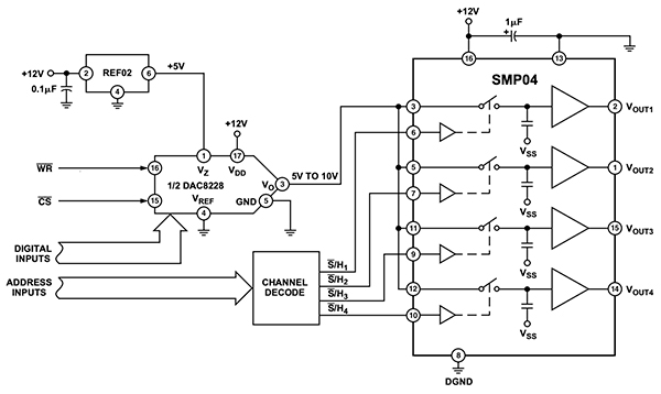 Figure 7: The Analog Devices SMP04 quad S&H contains four independent S&H circuits along with matching buffer amplifiers. The circuit shown uses the SMP04 being used to multiplex the output of a DAC into four channels. (Image source: Analog Devices)
In the Figure, the SMP04 is used to multiplex the output of a DAC, breaking the single DAC output into four multiplexed channels. S&H circuits can be used to selectively delay the DAC’s output until after the glitch, thereby smoothing the DAC output.
Multiple S&H circuits can be used to increase the throughput of an ADC by pipelining multiplexed inputs. Here, multiple S&Hs are connected in common to the multiplexer output. The ADC is connected to one S&H, which holds the input level for a conversion. The other S&Hs acquire other multiplexer channels, and in turn, connect to the ADC, while the first S&H is free to connect to another multiplexed channel. This pipelining technique eliminates the S&H acquisition time in the ADC signal path.
Many ADCs incorporate S&H or T&H circuits within their integrated package. An example is the Texas Instruments ADC121S021CIMFX, a 12-bit successive approximation register (SAR) ADC with built-in T&H that operates with sample rates in the range of 50 to 200 kilosamples per second (kS/s). It features a high-speed serial output bus which simplifies wiring layout (Figure 8).
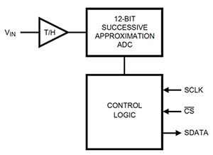 Figure 8: The Texas Instruments ADC121S021 is a 12-bit single-channel SAR ADC with a built-in T&H circuit. (Image source Texas Instruments)
This ADC is typical of many integrated ADC circuits in that it has an internal T&H, which simplifies pc board layout and helps minimize component count. External T&H circuits are used for special configurations such as differential input connections, multiplexed inputs, or when the ADC does not have an internal T&H or S&H circuit.
Conclusion
From audio recording to the most advanced IIoT or AI analysis, the most basic electronic function of converting an analog signal to a digital signal requires careful attention to S&H or T&H circuits. These are essential for minimizing voltage skew errors during the analog-to-digital conversion process as they hold the input voltage to the ADC constant during the conversion. The S&H can be internal to the ADC or external, but it must be in the signal path between the anti-aliasing low-pass filter and the ADC. As shown, there are many configurations—single, differential, or multiple devices per IC—to meet a variety of design applications. These applications extend to include preventing output transients or glitches caused by code transitions in DACs.
Recommended Reading

Disclaimer: The opinions, beliefs, and viewpoints expressed by the various authors and/or forum participants on this website do not necessarily reflect the opinions, beliefs, and viewpoints of DigiKey or official policies of DigiKey.


