Match the Right ADC to the Application
Contributed By DigiKey's North American Editors
2018-04-03
It’s an analog world controlled by digital computers. As such, designers of Internet of Things (IoT) devices need to efficiently convert analog values into sampled digital representations. While the simple answer may seem to be to just put an analog-to-digital converter (ADC) up front, not all ADCs are the same. Hence, designers need to understand the various topologies and how they map to the application.
For example, ADCs have been designed to optimize characteristics such as sampling rate, power consumption, and accuracy. This article will discuss the design requirements in the context of some common ADC architectures. It will then introduce applications that employ these architectures and show how they are implemented.
The role of an ADC
The ADC is a commonly used electronic integrated circuit or modular device that converts an analog signal, usually a voltage, into a series of sampled, discrete digital representations, or numbers. ADCs perform three distinct operations: sampling, quantization, and encoding. They form the heart of many common digital instruments such as voltmeters, oscilloscopes, and spectrum analyzers. They are also incorporated into the front-end of digital circuits that process analog signals coming from devices like microphones, accelerometers, photo sensors, and other transducers that need to have their output converted into the digital domain so that a microprocessor can work with the data.
There are many ADC architectures, or topologies, that have been developed to sample and digitize analog signals. Each form of the ADC has its own features, benefits, and weaknesses. The choice of a specific type of ADC for a given application is usually defined by the measurement requirements of speed, resolution, accuracy, power consumption, and physical size.
Key characteristics of an ADC
The first operation an ADC must perform is to sample the analog signal. Sampling is performed by a sample-and-hold or a track-and-hold circuit. The sampling or Nyquist theorem requires that the sample rate must be greater than twice the signal’s bandwidth in order to be able to reconstruct the analog signal from the digitized samples. Therefore, the first significant characteristic of the ADC is the sampling rate, which determines the maximum signal frequency component that can be digitized.
The ADC must quantize each sample, breaking the sampled voltage into a finite number of discrete amplitude levels. This characteristic is generally described as the number of bits of resolution. For instance, if a signal is broken down into 8 bits, it means that there are 28 or 256 discrete levels. A 16-bit ADC will break the voltage range into 65,536 quantization levels.
Both the resolution and the maximum sampling rate are determined by the ADC hardware. In general, the higher the ADC resolution, the more limited the maximum sampling rate.
The accuracy of an ADC is dependent on both the resolution and sampling rate. Resolution affects amplitude precision and accuracy. Other factors affecting the amplitude accuracy are the linearity of the quantization process and the effects of vertical noise. The sampling rate determines the timing precision and accuracy.
Physical size and power consumption are other attributes that depend on the circuit topology. They are major concerns for applications that have limited size or available power, such as IoT devices or battery powered, portable instruments. The physical size and power consumption are very dependent on the ADC topology.
Flash, direct, or parallel?
The most conceptually simple digitizer is the flash ADC. This may also be called a direct or parallel ADC (Figure 1).
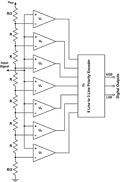
Figure 1: The flash ADC uses multiple comparators with uniformly incremented threshold voltages to convert an analog voltage into a digital number. This example shows a 3-bit ADC with a resolution of 8 levels. (Image source: DigiKey)
The input to the flash ADC usually comes from a sample-and-hold or a track-and-hold circuit where the analog input is sampled and held constant for the duration of the conversion. The sampled signal is applied to an array of analog comparators with threshold voltages that are uniformly spaced over the ADC’s input voltage range by a value equal to a single least significant bit (LSB). The output of each comparator changes state if the input voltage exceeds the threshold set for that comparator by the voltage divider. The example in the figure shows a 3-bit ADC which requires 7 comparators to produce 8 possible states.
In general, an N-bit flash converter requires (2N-1) comparators. The comparators produce what is called a “thermometer code.” The higher the input voltage, the greater the number of comparators reach their “1” state from bottom to top. This code is applied to a priority encoder which converts this code into a binary code.
The main advantage of the flash converter is speed. The conversion time only includes the delay of the comparator and the decoder. Flash converters with maximum sampling rates reaching 5 gigasamples per second (GS/s) are commercially available. The limiting factor for flash converter resolution is the number of comparators required. An 8-bit flash ADC would require 255 comparators.
This number increases by a factor of two for every bit of increased resolution. This means that the physical size of the ADC grows exponentially with resolution. This leads to the other limitation, which is the power required by the flash converter. This limits its usage to line powered applications. The practical limit to flash resolution is about 8 bits.
Binary encoding
The binary output of the ADC can be encoded in several ways. If the signal being converted is unipolar, then it is usually encoded as a unipolar straight binary code. This code represents a zero value as all zeros (0000…) and the maximum input value as all ones (1111…).
If the signal is bipolar, then it is generally represented as either offset binary or two’s complement binary as detailed using a 4-bit example (Table 1).
|
Table 1: Common binary encoding for bipolar digital signals. Two’s complement binary is most widely used by microprocessor or math processors. (Image source: DigiKey)
Two’s complement binary coding is the type of coding used by most microprocessor or math processor based systems as it facilitates arithmetic operations.
Pipelined, sub-ranging, and two-step ADCs
The number of comparators in a flash converter can be decreased by breaking the conversion up into two or more steps and converting a smaller number of bits per stage. If the flash ADC is split into two sections it is called a two-step or sub-ranging ADC. If it is broken into more than two sections it is referred to as a pipelined ADC. A two-step ADC can still sample at hundreds of megasamples per second (MS/s) (Figure 2).
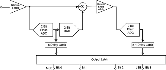
Figure 2: A functional block diagram of a 4-bit, two-step, or sub-ranging ADC shows it breaks the 4-bit converter into two 2-bit converters to decrease the number of comparators. (Image source: DigiKey).
This two-step converter breaks the 4-bit converter, which would require 15 comparators, into two 2-bit sections. Each section uses three comparators for a total of six comparators. The converter operates by converting the two most significant bits (MSB) first. The digital output of the first section includes a digital-to-analog converter (DAC) to convert the signal to analog and subtract it from the input signal.
The resultant difference is amplified and used to convert the two LSBs. The combined results are captured in the output latches. The conversion process is repeated twice so the maximum sampling rate will be lower than that of the flash converter. The Analog Devices AD9203ARUZRL7 is an example of a 10-bit, 40 MS/s pipelined ADC that solves the problem of converting from analog to digital at high speed.
Successive approximation register (SAR) ADCs
When the application requires greater resolution, and not necessarily the speed of the flash or pipelined ADC, then the successive approximation register (SAR) converter is a good choice (Figure 3). SAR ADCs operate at 12 to 16 bits, with sample rates as high as 1 to 2 MS/s.
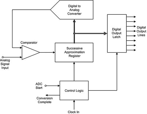
Figure 3: The SAR ADC provides good resolution with low to moderate power requirements. (Image source: DigiKey)
Like the flash ADC, the SAR ADC is preceded by a sample-and-hold or track-and-hold circuit to maintain the sample value for the duration of the conversion process. The signal from the sample-and-hold is applied to a comparator. The successive approximation register starts at mid-range and converts the value to an analog voltage with the DAC.
This ‘guess’ voltage is compared with the signal input at the comparator. If the comparator output stays low, the register value is incremented by one quarter of the range. Essentially the register value is lowered or raised in factors of two steps until the comparator indicates that the DAC converted register content equals the input signal voltage. When that occurs, the converter issues the “conversion complete” signal and latches the digital value into the output latch.
The conversion time is proportional to the ADC resolution, which is set by the length of the register. SAR ADCs provide good resolution with low to moderate power requirements. An example of a low-cost, low-power SAR is the MAX11665AUT-T from Maxim Integrated. It is a 12-bit, 500 kilosamples per second (kS/s) SAR ADC, making it well matched to digitizing sensor outputs.
Integrating dual slope ADC
Integrating ADCs offer high resolution while minimizing the effects of noise. The dual slope ADC is the most common integrating ADC (Figure 4).
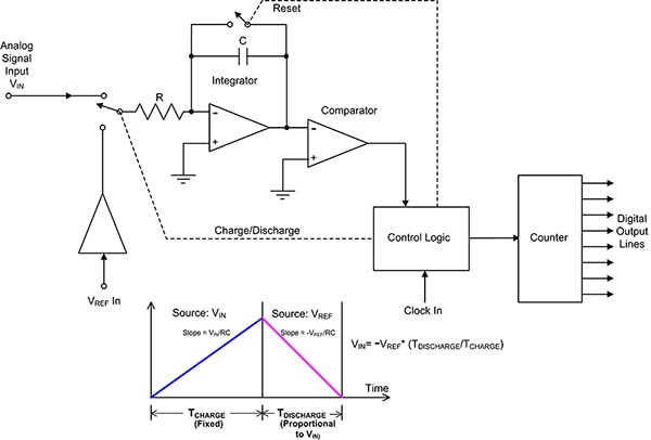
Figure 4: The block diagram of a dual slope integrating ADC including a graph showing how the charge/discharge timing is used to determine the unknown input voltage. (Image source: DigiKey)
Initially, the input is connected to the integrator. The capacitor, C, is charged by the input signal for a fixed time. At the completion of the charge time, the integrator is connected to the reference voltage. This discharges the capacitor to zero as determined by the comparator. A counter measures the time it takes to discharge the capacitor. The time is proportional to the input voltage impressed on the capacitor during the charge cycle. A simple relationship based on the known charge time and measured discharge time allows calculation of the input voltage.
Because the signal input is applied to an integrator, the effect of any noise signal is minimized by the averaging effect of the integrator. The dual slope converter is ideal for high resolution applications requiring high accuracy. Resolutions of 12 to 16 bits are common, with maximum sample rates up to 100 KS/s.
The most well-known application for dual-slope ADCs is digital voltmeters (DVM or DMM). The Maxim Integrated model ICL7109CPL+ 12-bit ADC with tri-state outputs is a dual-slope converter intended for measuring analog signals like pressure, speed, or flow, at rates of up to 30 times per second.
The sigma delta ADC: high resolution at low frequencies
The sigma delta ADC offers the highest resolution (16 to 24 bits) for low frequency signals. Like the dual-slope ADC, it is another type of integrating digitizer (Figure 5). The input signal is applied through a summer to the integrator. The output of the integrator is applied to a latched comparator where it is compared with a zero volt (ground) signal. If the integrated output is not zero, the comparator output is fed back to bring the integrator output closer to zero. This process is repeated at the converter clock rate until the integrator output reaches zero. The comparator output forms a serial data stream which is the digital output of the converter.
The sigma delta ADC is sampled at a rate much higher than that required for the designed sample rate.
Note in the figure the converter clock is faster than the output sample clock by a factor K. The extra samples from this ‘over sampling’ are used to provide digital filtering of the converter output. A decimator restores the output sample rate to the specified sample clock rate.
The Analog Devices model AD7734BRUZ ADC is a 24-bit, 4-channel, sigma delta digitizer intended for process and industrial control applications.
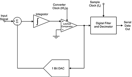
Figure 5: A sigma delta ADC is widely used for high-resolution digitization of low-frequency signals for audio, process and industrial control applications. (Image source: DigiKey)
A summary of the resolution and maximum sampling rate for the five ADC types discussed is provided in Table 2.
|
Table 2: ADC operating characteristics for the five ADC types discussed in this article. (Image source: DigiKey)
Topology selection example
Consider an application to digitize the signals from a portable ultrasonic range finder which uses a 40 kHz transducer. Target reflections are -40 dB (1/100) of the transmitted pulse amplitude.
The signal must be sampled at a minimum of twice the 40 kHz signal frequency. It is better to sample it at four or more times 40 kHz, so the desired sample range is 160 kHz or greater. It is a good idea to set a resolution that is at least ten times the expected 40 dBm, so that would be 60 dB. The general rule of thumb is that every 6 dB requires 1 bit of resolution, so a 10-bit or more ADC would be required. Additionally, this is a portable instrument making power consumption a consideration. Consulting Table 2, the successive approximation converter would be the best choice. The MAX11665AUT-T from Maxim Integrated, mentioned earlier as example of a SAR ADC, would be a good match for this application.
Conclusion
As both cannot be achieved simultaneously, the choice of an ADC is primarily a tradeoff between maximum sample rate and resolution. Other considerations, such as physical size and power consumption, play a role depending upon the application and should be given due weighting in the selection process.

Disclaimer: The opinions, beliefs, and viewpoints expressed by the various authors and/or forum participants on this website do not necessarily reflect the opinions, beliefs, and viewpoints of DigiKey or official policies of DigiKey.


