Sometimes the More Expensive ADC is the Most Cost Effective
Contributed By DigiKey's North American Editors
2017-11-15
In portable medical devices and industrial automation, where temperature measurement, pressure measurement, and industrial process control are involved, 12 bits is considered enough to make good decisions. However, when factoring in a complete multi-sensor system design, 24-bit converters may be the more cost-effective option, and here’s why.
When starting out on a system design, designers typically proceed to develop a 12-bit system, starting with a 12-bit converter and then developing the front-end analog chain. However, the front-end circuitry involves multiple amplifiers, adding design time, space, complexity and in the end, greater overall cost.
There is a better way. This article briefly discusses how to use an 8-channel, 24-bit converter to replace all those 12-bit signal chains. The Analog Devices AD7124-8BCPZ-RL7 8-channel, low-noise, low-power analog-to-digital converter (ADC) will be used as an example.
The typical 12-bit multi-sensor design
Creating portable sensing systems, the designer takes the fact that they need a 12-bit, 14-bit, or 16-bit system and proceeds to develop that system. The design effort starts with the front-end analog chain and the appropriate successive approximation register (SAR) ADC.
It is reasonable to find some system that integrates multiple sensors. A good example is a patient monitor that collects temperature, weight, blood oxygen, and a verbal statement (Figure 1).
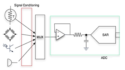
Figure 1: A patient monitor with voice recorder is a good example of a system with multiple sensors. (Image source: DigiKey)
A common 12-bit sensing system performs a high-side or low-side system current measurement. In such a system, a sub-ohm value resistor (RSHUNT) is used to sense the system current by converting that current to a voltage (Figure 2). This shows a standard high-side current sensing circuit that ultimately converts the system’s current to a usable digital word using the SAR-ADC.
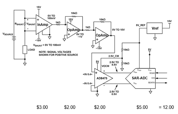
Figure 2: A typical 12-bit high-side current sensing circuit shows a SAR-ADC converting the current being sensed by RSHUNT into a usable digital word. (Image source: DigiKey)
In Figure 2, the sub-ohm shunt resistor is across an instrumentation amplifier (InAmp) that is capable of sensing voltages near the power supply voltage. The output of the InAmp is in a range of 0 to 100 millivolts (mV). For a 12-bit system, the least significant bit (LSB) size at this point is 24.4 microvolts (mV). Two amplifiers then gain this signal, both by a gain of -10 V/V. At this point in the circuit, the output range of the signal is 0 to 10 volts. The signal then goes to the fully differential amplifier (FDA). This amplifier appropriately provides a differential output for the SAR-ADC differential input pins, where the LSB size is 1.22 mV.
The cost analysis below, will use 1000 piece pricing estimates. Back to the front end of Figure 2, the InAmp device is a specialty device as it is capable of accurately sensing the small input signal near the power supply. The trade-off for this circuit portion is that RSHUNT must be as low as possible in an attempt keep the power supply to the load as constant as possible. For this type of specialty device, the cost estimate is ~$3.00.
Following the InAmp, there are two operational amplifiers (OpAmps). Preferably, both OpAmps are part of a dual configuration. These amplifiers must have low input bias current, offset voltage and noise. The input bias current and offset voltages will add to the offset error as the signal progresses to the SAR-ADC. High amplifier noise will compromise the signal-to-noise ratio (SNR) of the signal chain. For this type of dual amplifier, the cost estimate is ~$2.00.
The FDA receives the output signal of the OpAmps. The function of the FDA is to change the single-ended signal to a differential output, multiply the full-scale range by 0.4 V/V, and implement a level shift to 2.5 volts. For the FDA, the cost estimate is ~$2.00.
Finally, the SAR-ADC receives the FDA’s differential signal. This application circuit measures the current flowing through the load. This high-side current sensor circuit requires no more than a 12-bit granularity of the conversion results. For Figure 2, the typical cost for a 12-bit SAR-ADC is ~$5.00.
The front-end circuitry in Figure 2 involves multiple chips including four amplifiers, thereby adding design time, space, complexity and in the end, cost. In our example, the front-end cost is ~$7.00.
This process can be performed on numerous sensing circuits, but this instance will use a 24-bit sigma-delta (∑∆) converter from Analog Devices.
Replacing 12-bit with the 24-bit converter
There is a better way to implement the Figure 2 circuit. The SAR-ADC function requires signal conditioning circuitry, an analog multiplexer and an amplifier driver. The alternative is to switch the converter to a ∑∆-ADC (Figure 3).
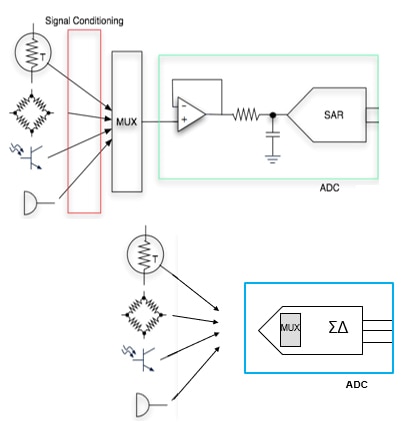
Figure 3: Sensing-circuit block diagrams: the top diagram has a SAR-ADC as the converter. The bottom diagram has a ∑∆-ADC as the converter. (Image source: DigiKey)
Figure 3 illustrates the fundamental difference between the SAR-ADC and ∑∆-ADC signal paths. The SAR-ADC signal path requires signal conditioning which prepares the small sensor signals to meet the converter’s input range. The sensor connections in the ∑∆-ADC signal path are connected directly to the converter’s inputs.
Using the ∑∆-ADC signal chain, a designer can forget the analog gain stages and remove the level-shift circuits. This circuit will continue to use the InAmp because it offers protection capability for over-voltage events, however, all of the other amplifiers are unnecessary (Figure 4).
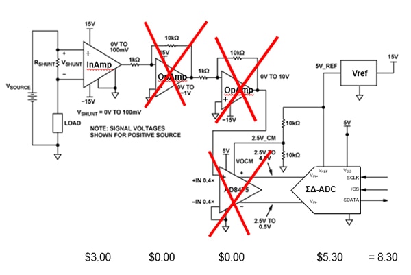
Figure 4: High-side current sensing using a ∑∆-ADC showing elements that have been replaced. (Image source: DigiKey)
All that is of interest with the above system is an LSB size of 24.4 mV. For accuracy’s sake, it’s worth dividing that LSB size by two, to give 12.2 mV. The number of bits needed for a 5 V system is easy to calculate as 1.44*ln(full-scale-range/LSB). For this circuit, the number of bits is 18.6, rounded up to 19 bits.
Again, 1000 piece pricing estimates are used for this cost analysis. Back to the front end of Figure 4, we will still use the InAmp device. For this type of specialty device, the typical cost is still ~$3.00.
Following the InAmp, the two amplifiers are eliminated. This saves ~$2.00. The FDA is also eliminated because the ∑∆-ADC does the level-shift function digitally. Once again, this will save ~$2.00.
Finally, the SAR-ADC receives the FDA’s differential signal. This application circuit measures the current flowing through the load. This high-side current sensor circuit requires no more than a 12-bit granularity of the conversion results. Referring to Figure 2 again, the typical cost for a 24-bit ∑∆-ADC is ~$5.30.
The removal of the front-end circuitry in Figure 4 reduces circuit complexity and cost. The only analog survivor in this circuit is the InAmp. In this example, the front-end cost is now ~$3.00.
Full capability of ∑∆-ADC
This signal has now been put into a 24-bit system, with no gain. In this 24-bit system, the LSB size is equivalent to having a gain of 4098 for the 12-bit system (Figure 5).
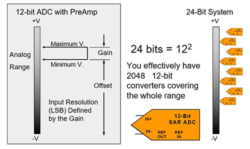
Figure 5: In this 24-bit system, the LSB size is equivalent to having a gain of 4098 for the 12-bit system. (Image source: DigiKey)
Although the input range to the ∑∆-ADC for a particular sensor is small, the converter is able to produce 12-bit resolution for all sensors, minus the signal conditioning stages.
So let’s put a little reality in this approach. Upon finding a 24-bit ∑∆-ADC with a full-scale range of 5 V, designers will have the opportunity to eliminate their signal chain elements. If they take this approach a little further, they can use a ∑∆-ADC that has internal programmable gain amplifiers (PGAs), allowing the addition of the analog signal chain elements inside the ∑∆-ADC (Figure 6).
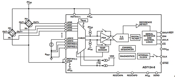
Figure 6: The AD7124-8 24-bit ∑∆-ADC with 4 of the 16 input pins. (Image source: Analog Devices)
The eight differential input AD7124-8, 24-bit ∑∆-ADC is a low-noise solution containing programmable gain (1 to 128), an internal voltage reference, and an internal clock oscillator. This device is well suited to eliminate the burdensome analog signal conditioning circuitry shown in Figure 2.
Conclusion
This article briefly discussed why it’s often better to use a 24-bit converter instead of multiple 12-bit devices, and how to lower the cost and complexity of the analog front end for multi-sensor devices.
The Analog Devices AD7124-8BCPZ-RL7 8-channel, low noise, low power, ∑∆ ADC, was used as an example. This device will also remove the need for a PGA and a voltage reference.
References
- "Accuracy comes in many flavors", Baker, Bonnie, EDN, January 8, 2004, pg. 22

Disclaimer: The opinions, beliefs, and viewpoints expressed by the various authors and/or forum participants on this website do not necessarily reflect the opinions, beliefs, and viewpoints of DigiKey or official policies of DigiKey.


