A Review of Zero-Voltage Switching and its Importance to Voltage Regulation
Contributed By Electronic Products
2014-08-05
Step-down (“buck”) DC-DC voltage regulator circuit design is getting harder because power density (W/m3) is rising, DC power supply voltage levels are rising, and silicon voltage demands are dropping in order to increase efficiency. The difference between the supply voltage and that required by the silicon creates a big drop across the regulator, increasing switching losses and ultimately limiting the device’s switching frequency.
For example, a process-control system may call for regulation from 24 to 3.3 V – a gap that would typically have to be covered using two regulation stages, thereby increasing board space, cost, and reliability issues. Moreover, limited switching frequency is a drawback because it forces engineers to use larger magnetic and other passive components for filtering circuits, increasing the solution size and working against power density.
One solution enabling a return to faster switching frequency at higher input voltage and voltage drop is Zero Voltage Switching (ZVS). This technique, like virtually all contemporary switching voltage regulators, uses pulse width modulation (PWM)-based operation, but with an additional separate phase to the PWM timing to allow for ZVS operation. ZVS enables the voltage regulator to engage “soft switching”, avoiding the switching losses that are typically incurred during conventional PWM operation and timing.
This article describes ZVS and explains its advantages.
Hard-switching losses
Most contemporary non-isolated buck voltage regulators incur high-switching losses due to the simultaneous occurrence of high-current and -voltage stress imposed on the regulator’s integrated metal oxide semiconductor field-effect transistor (MOSFET) switch during the turn-on and turn-off transitions. These losses increase with switching frequency and input voltage and limit maximum frequency operation, efficiency, and power density.
Hard switching occurs during the overlap between voltage and current when switching the MOSFET on and off. Voltage regulator manufacturers try to minimize the overlap to in turn minimize the switching losses by increasing the rate of change of current (di/dt ) and voltage (dv/dt) in the switching waveform. Figures 1 and 2 illustrate where the switching losses occur and show an actual switching waveform with fast-changing voltage designed to minimize these losses.
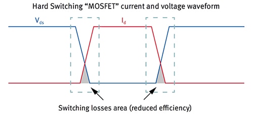
Figure 1: Voltage regulator losses occur during voltage/current overlap when the MOSFET switches (Courtesy of Infineon Technologies).
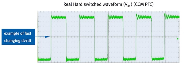
Figure 2: Manufacturers increase dv/dt to minimize overlap and improve efficiency (Courtesy of Infineon Technologies).
The downside of fast switching is an increase in electromagnetic interference (EMI) emanating from the voltage regulator circuitry.
One way to minimize EMI effects, while still taking advantage of fast switching to enhance efficiency, is to select a switching regulator that employs an improved hard-switching technique called quasi-resonant switching (also known as “valley” switching). Infineon Technologies offers a range of power MOSFETs, such as its CoolMOS series, for quasi-resonant flyback switching voltage regulators.
During quasi-resonant switching the MOSFET is turned on when the voltage across drain and source is at a minimum (in a valley) in order to minimize the switching losses. This allows the device to operate with a more modest rate of change in voltage or current, and thus reduces EMI. Another positive side effect of quasi-resonant switching is that because switching is triggered when a valley is detected, rather than at a fixed frequency, a degree of frequency jitter is introduced, spreading the RF emission spectrum and further reducing EMI.
Quasi-resonant switching does have the disadvantage of inducing higher losses at light loads, but the problem is eliminated in modern devices by employing a frequency-clamp circuit to limit the maximum operating frequency. Figure 3 shows a quasi-resonant switching waveform for a flyback converter where the MOSFET is switched in the valleys.
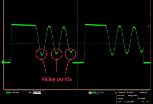
Figure 3: Quasi-resonant switching waveform for a flyback converter (Courtesy of Infineon Technologies).
Soft switching at zero voltage
Quasi-resonant switching is a good technique for improving voltage-converter efficiency, but things can be further improved by implementing full soft switching. During soft switching the voltage falls to zero (rather than just a minimum) before the MOSFET is turned on or off, eliminating any overlap between voltage and current and minimizing losses. (The technique can also be used to switch the MOSFET when current, rather than voltage, reaches zero. This is known as Zero Current Switching (ZCS).) An additional advantage is that the smooth switching waveforms minimize EMI (Figure 4).
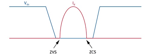
Figure 4: Soft-switching MOSFET current and voltage waveform (Courtesy of Infineon Technologies).
Soft switching (ZVS) can best be defined as conventional PWM power conversion during the MOSFET’s on-time but with “resonant” switching transitions. The technique can be considered PWM power utilizing a constant off-time control which varies the conversion frequency, or on-time to maintain regulation of the output voltage. For a given unit of time, this method is similar to fixed-frequency conversion using an adjustable duty cycle.
Regulation of the output voltage is achieved by adjusting the effective duty cycle (and thus on-time), by varying the conversion frequency. During the ZVS switch off-time, the regulator’s L-C circuit resonates traversing the voltage across the switch from zero to its peak and back down again to zero when the switch can be reactivated, and lossless ZVS facilitated. The MOSFET transition losses are zero––regardless of operating frequency and input voltage––representing a significant savings in power, and a substantial improvement in efficiency (Figure 5). Such attributes make ZVS a good technique for high-frequency, high-voltage converter designs.¹
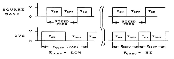
Figure 5: Conventional PWM employs a fixed frequency, but varies the duty cycle to achieve regulation; in contrast, ZVS varies the conversion frequency (which in turn alters the on-time) to maintain output voltage (Courtesy of Texas Instruments).
Two other advantages of ZVS are that it reduces the harmonic spectrum of any EMI (centering it on the switching frequency) and allows higher frequency operation resulting in reduced, easier-to-filter noise and the use of smaller filter components.
One downside is that there is no guarantee (particularly at high frequencies) that the MOSFET has dissipated all its energy before being switched off. In the long term this “stored” energy can cause component failure, especially in a fast-switching voltage regulator. Power-module makers overcome this problem by adding a fast body diode in parallel with the switch to make sure all the energy is drained from the transistor (Figure 6).²
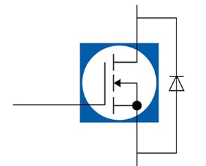
Figure 6: ZVS topologies typically include a fast-body diode in parallel with the MOSFET to ensure all energy is drained from the transistor (Courtesy of Infineon Technologies).
Zero-voltage switching in action
Figure 7 shows a schematic for a ZVS buck topology. This circuit is identical to a conventional buck regulator except for an added clamp switch connected across the output inductor. The switch is added to allow energy stored in the output inductor to be used to implement ZVS.
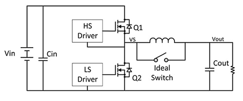
Figure 7: ZVS buck topology (Courtesy of Vicor).
The ZVS buck converter operates in three main states. They are defined as Q1 on phase, Q2 on phase, and clamp phase. Q1 turns on at zero current and when the drain-to-source voltage is nearly zero. Current ramps up in the MOSFET and the output inductor to a peak current determined by the on-time of Q1, the voltage across the inductor, and the inductor value. During the Q1 on phase, energy is stored in the output inductor and charge is supplied to the output capacitor. During the Q1 on phase, the power dissipation in Q1 is dominated by MOSFET on-resistance and the switching loss is negligible.
Next, Q1 turns off rapidly followed by a very short body diode conduction time (adding negligible power dissipation). During the current commutation to the body diode, Q1 does experience turn-off losses in proportion to the peak inductor current. Next, Q2 turns on and the energy stored in the output inductor is delivered to the load and output capacitor. When the inductor current reaches zero, the synchronous MOSFET Q2 is held on long enough to store some energy in the output inductor from the output capacitor.
Once the controller has determined that there is enough energy stored in the inductor, the synchronous MOSFET turns off and the clamp switch turns on, clamping the VS node to VOUT. The clamp switch isolates the output inductor current from the output while circulating the stored energy as current in a nearly lossless manner. During the (very small) clamp-phase time the output is supplied by the output capacitor.
When the clamp phase ends, the clamp switch is opened. The energy stored in the output inductor resonates with the parallel combination of the Q1 and Q2 output capacitances, causing the VS node to ring towards VIN. This ring discharges the output capacitance of Q1, diminishes the gate-to-drain (Miller) charge of Q1 and charges the output capacitance of Q2. This allows Q1 to turn on in a lossless manner when the VS node is nearly equal to VIN.³
Power modules with ZVS
Vicor is a prime example of a company that has embraced ZVS topology. The company has produced a white paper explaining how ZVS works in non-isolated Point-of-Load (POL) buck-regulator applications.
The company’s Cool-Power ZVS buck regulators form a family of high-density, isolated DC-DC ZVS converter modules integrating controller, power switches, planar magnetics, and support components in a high-density surface-mount package.
These power modules are offered in three input-voltage operating ranges; 48 V for communication applications, 28 V for rugged high-temperature applications, and 24 V for industrial applications. The modules are equipped with a variety of programmable features, including output voltage trimming and programmable soft-start capability (Figure 8).
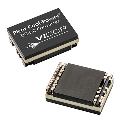
Figure 8: Vicor’s Cool-Power ZVS buck regulators form a family of high-density, isolated DC-DC ZVS converter modules.
The company claims that ZVS improves efficiency by up to 12 percent compared with competitive devices (Figure 9).
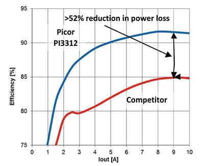
Figure 9: Efficiency curves for Vicor’s Picor PI13312 ZVS topology compared with competitor’s device.
Other manufacturers offer modular controllers that can be used for ZVS control strategies for full-bridge converters. For example, Linear Technology supplies the LTC3722 for this purpose. This phase-shift PWM controller provides all of the control and protection functions necessary to implement a high-efficiency ZVS full-bridge power converter. Adaptive ZVS circuitry delays the turn-on signals for each MOSFET independent of internal and external component tolerances. The chip can be used as the basis for voltage regulators with up to 93 percent efficiency.
For its part, Texas Instruments (TI) offers a DC-DC switching controller for ZVS regulation, the UCC28950. This controller can implement supervision of a full-bridge converter with active control of the synchronous rectifier output stage. The primary-side signals allow programmable delays to ensure ZVS operation over wide-load current and input-voltage range, while the load current tunes the secondary-side synchronous rectifier switching delays, maximizing system efficiency.
Driving up energy density
High-density regulators are struggling to keep up with the demands of modern electronic systems primarily due to switching losses hindering performance within the regulator MOSFETs. ZVS addresses these losses and can be applied to most power-conversion designs, but is most advantageous to those operating from a high-voltage input. Significant improvements in efficiency can be obtained in high-voltage, half- and full-bridge ZVS applications when compared to their PWM-controlled equivalents.
Moreover, ZVS technology allows the use of switches with lower-voltage ratings, because there is no transient overvoltage, and the reverse voltage applied to the primary switches is limited to the peak input voltage, at most. This frees up engineers to use components with superior characteristics such as lower conduction losses, lower driving currents, and higher energy density.
For more information on the parts discussed in this article, use the links provided to access product information pages on the Digi-Key website.
References:
- “Zero Voltage Switching Resonant Power Conversion,” Bill Andreycak, Texas Instruments, 1999.
- “CoolMOS™ Benefits in both Hard and Soft Switching SMPS topologies,” Infineon Technologies, November 2011.
- “High-Performance ZVS Buck Regulator Removes Barriers to Increased Power Throughput in Wide Input Range Point-Of-Load Applications,” C. R. Swartz, Vicor, August 2012.
Disclaimer: The opinions, beliefs, and viewpoints expressed by the various authors and/or forum participants on this website do not necessarily reflect the opinions, beliefs, and viewpoints of DigiKey or official policies of DigiKey.


