Innovative Insights: CMOS Inverter Basics Unveiled!
2024-08-30 | By DWARAKAN RAMANATHAN
Introduction:
The CMOS inverter is a cornerstone in modern digital electronics, playing a pivotal role in numerous electronic devices and circuits. Understanding its operation and applications is essential for both beginners and experienced engineers alike. Let’s delve into the intricacies of the CMOS inverter, exploring its principles, characteristics, and practical uses.
What does CMOS stand for?
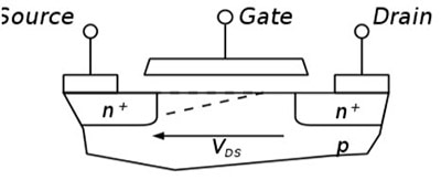
CMOS stands for Complementary Metal-Oxide-Semiconductor, a technology used to make integrated circuits (ICs). In CMOS, both n-type and p-type MOSFETs (Metal-Oxide-Semiconductor Field-Effect Transistors) are used to create digital and analog circuits on a single chip. CMOS technology is popular because it has low power consumption, high noise resistance, and high packing density. This makes it ideal for devices like microprocessors, memory chips, and digital signal processors. In a CMOS circuit design, there are two networks: the pull-up network (using P Channel MOSFETs) and the pull-down network (using N Channel MOSFETs). The pull-up network pulls the output voltage to a logic HIGH (like 5V or 2.5V), while the pull-down network pulls the output to a logic LOW (0V).
CMOS Inverter:
A CMOS inverter is designed using Complementary Metal-Oxide-Semiconductor. To learn more about MOSFETs, Click here. Complementary Metal-Oxide-Semiconductor (CMOS) technology uses both NMOS (n-channel) and PMOS (p-channel) transistors. This combination results in low power consumption, high noise immunity, and high packing density. The CMOS inverter, which consists of these complementary transistors, showcases these benefits and acts as a basic building block in digital integrated circuits.

How does it work?
There are two types of MOSFETs present here. One is used to charge the output capacitor or Vout, and another is used to discharge the capacitor or Vout. (Note: The capacitor is imaginary and not depicted in the above picture).
- Charging:
This happens when the input of the inverter is low. When the input of the inverter is low (Vin = 0), the PMOS is turned on, and the NMOS is turned off. So, The Vout is directly connected to the Vdd, making the output logic HIGH.

- Discharging:
This happens when the input of the inverter is High. When the input of the inverter is high (Vin = 5V), the PMOS is turned off, and the NMOS is turned on, connecting the Vout to the ground. So, the output is pulled down to Zero Volts or Logic LOW.

Characteristics of CMOS Inverter:
The CMOS inverter has several important features: high input impedance, low output impedance, and equal rise and fall times. These characteristics give it excellent noise immunity, fast switching speeds, and low power consumption, making it ideal for many digital applications. Additionally, the CMOS inverter's voltage transfer characteristics show that it can provide a full range of output voltages (rail-to-rail) while maintaining a wide noise margin, ensuring reliable performance across different voltage levels and environmental conditions.
Voltage transfer characteristics of CMOS Inverter:
The voltage transfer characteristics (VTC) of a CMOS inverter show how the output voltage (Vout) changes in response to the input voltage (Vin). This graph highlights the relationship between input and output voltages and gives important insights into the inverter's performance. In an ideal CMOS inverter, the VTC displays a sharp transition between the logic high (1) and logic low (0) states. This transition happens at a specific threshold voltage, called Vth, where the inverter switches between the conducting states of the n-channel and p-channel transistors.

VOH - VOLTAGE OUTPUT HIGH
VOL - VOLTAGE OUTPUT LOW
VIL - VOLTAGE INPUT LOW
VIH - VOLTAGE INPUT HIGH
Applications:
CMOS inverters are highly versatile and find applications across a broad spectrum of electronic systems. They are fundamental components in digital logic circuits, memory circuits, microprocessors, and more. From basic logic gates to complex arithmetic circuits and digital signal processors (DSPs), CMOS inverters serve as essential building blocks, enabling the creation of efficient and dependable electronic systems. Furthermore, their incorporation into Complementary Metal-Oxide-Semiconductor integrated circuits (CMOS ICs) supports the development of advanced technologies like microcontrollers, Application-Specific Integrated Circuits (ASICs), and System-on-Chip (SoC) solutions. This integration enhances performance, lowers power consumption, and increases reliability, driving innovation in various fields of electronics.
Conclusion:
The CMOS inverter stands as a cornerstone in modern digital electronics, combining performance, efficiency, and versatility. Understanding its operational principles, characteristics, and applications empowers engineers and enthusiasts to leverage CMOS technology in designing innovative electronic systems. Whether applied in consumer electronics, telecommunications, or industrial automation, the CMOS inverter remains pivotal in driving forward electronic innovation and shaping the future of digital technology.