Design an Effective Front-End Filter for Wearable Medical Instruments
資料提供者:DigiKey 北美編輯群
2017-08-31
Converting analog sensor signals to the digital domain is standard practice with wearable patient monitoring equipment. However, designers must be aware that these applications depend on a system that produces reliable, repeatable results, albeit in their noisy environments. Noise filtering techniques are a critical portion of the solution circuit.
Historically, the filtering process resided solely in the analog domain. More recently, with the advent of the microcontrollers and more sophisticated signal processors, there is a temptation to move the filtering function completely into the digital domain: but buyer beware. There are advantages and disadvantages to doing this.
This article briefly discusses analog domain versus digital domain noise filtering advantages and disadvantages. It uses two designs as examples of each filtering approach. Design number one uses the STMicroelectronics TSX7191IYLT low-power, precision, rail-to-rail, 9.0 MHz operational amplifier (op amp) to implement the analog low-pass filter.
Design number two uses Microchip Technology’s PIC18LF25K40T-I/MV, low-power, high-performance microcontroller with XLP Technology to implement the coded finite impulse response (FIR) filter.
Analog versus digital filtering
The analog filtering approach uses a low-pass or an anti-aliasing filter placed prior to the analog-to-digital converter (ADC). Adding this filtering function before the ADC effectively reduces unwanted noise, but adds cost and consumes pc board real estate (Figure 1).
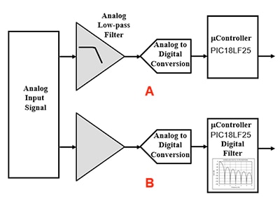
Figure 1: Analog-to-digital signal path with analog filtering (A) or digital filtering using the PIC18LF25K40T-I/MV MCU (B). (Image source: DigiKey)
The digital solution, which follows the ADC, uses averaging methods to reduce noise. The addition of filtering into the processor’s code is basically ‘free’ as the processor is already in the circuit to perform other functions. There is a minor cost for this digital-based filtering function in terms of coding time, but a more serious consequence of using digital filtering is it’s limited ability to attenuate the aliased signals.
The Nyquist Theorem
Almost any discussion of signal conversion and filtering must consider the Nyquist Theorem, also known as the sampling theorem. This relates to an ADC’s digitization process, stipulating that the sampling rate of the ADC must be at least 2x the frequency of the signal being sampled, or aliasing will occur. This sampling rate is the time required for the converter to sample, acquire, digitize, and prepare for the next conversion. It’s also called the converter’s throughput rate.
With multiple samples, the ADC faithfully reproduces the analog input signal in terms of magnitude, however it also modifies the frequency domain above ½ of the ADC’s sampling frequency, according to the formula FALIASED = |fIN – Nfs| (Figure 2).
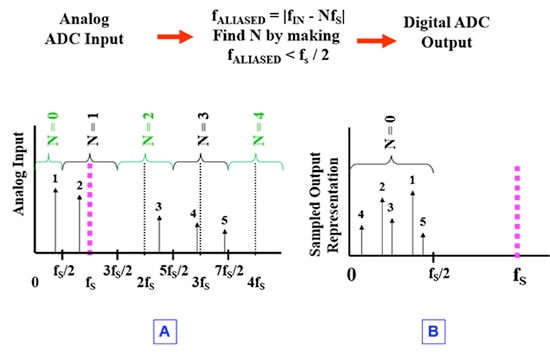
Figure 2: When the signal bandwidth is less than half of the sample rate, the original signal can be reconstructed. If the signal bandwidth is greater than half of the sample rate, the original signal frequency is modified. (Image source: DigiKey)
Prior to the ADC, the ADC’s sampling frequency (fS) determines the Nyquist divisions (Figure 2.A). The frequency range of N = 0 is from DC to fS/2. The N = 1 frequency range encompasses ± fS/2 around fs. The N = 2 frequency range encompasses ± fS/2 around 2fs. This pattern continues with rising frequency. The delineations of the analog frequency ranges lead to the frequency placement of signals after digitization.
For instance, Signal 1 is perfectly preserved in terms of magnitude and frequency as the analog signal is digitized through the ADC (Figure 2B). This is because the frequency of Signal 1 is between DC and the sampling frequency divided by two (fS/2). However, for Signals 2 through 5, the ADC conversion no longer preserves the analog input to digital output frequency relationship.
In all cases, the ADC conversion (ideally) preserves the signal magnitude. The frequency conversion of Signal 2 is equal to |f2 – fS|, where f2 is Signal 2’s frequency. Notice that in the digital domain, f2 is closer to DC than to fS/2.
The frequency conversion of Signal 3 is equal to |f3 – 2fS|, where f3 is Signal 3’s frequency. Notice that in the digital domain, f3 is half way between DC and fS/2. Similarly, the frequency conversion of Signal 4 is equal to |f4 – 3fS|, where f4 is Signal 4’s frequency. Notice that in the digital domain, f4 is very close to DC. The frequency conversion of Signal 5 is equal to |f5 – 3fS|, where f5 is Signal 5’s frequency. Notice that in the digital domain, f5 is even closer to fS/2.
After the frequency rich analog signal travels through the ADC, the digital output is truly frequency rich, however, the frequencies all clutter between DC and fS/2. It is impossible to recover the original frequency content and further discern between “good” and “bad” signals.
Analog low-pass filter
An easy solution to the above problem is to include an analog low-pass filter in the signal chain. This filter sits at the input of the ADC. The low-pass filter attenuates higher frequency signals. A generic frequency response of this low-pass filter allows lower frequency signals to pass through, while attenuating higher frequency signals (Figure 3).
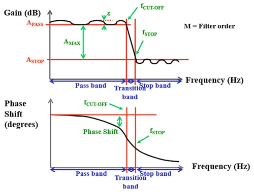
Figure 3: Generic low-pass frequency response showing higher frequency attenuation. (Image source: DigiKey)
The gain curve in the pass band region can be flat or have a slight ripple. At fCUT-OFF, or the end of the pass-band region, the filter starts into the transition band. The speed of signal attenuation, or roll-off rate, is dependent on the filter approximation type and filter order. Examples of filter approximation types are:
- Bessel
- Butterworth
- Chebyshev
- Inverse Chebyshev
- Traditional Gaussian
- Linear phase
The order of a low-pass filter defines the number of poles. For instance, a 4th order filter has four poles, indicating that there are four capacitors in the circuit.
The low-pass filter can be implemented in many ways. Common implementations are the Sallen-Key and the multiple feedback (MFB) circuits (Figure 4).
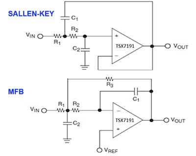
Figure 4: Sallen-Key and multiple feedback (MFB) low-pass filter implemented using STMicroelectronics’ TSX7191IYLT op amp. The Sallen-Key is non-inverting, the MFB is inverting. (Image source: DigiKey)
The implementation of gain of the Sallen-Key low-pass filter is non-inverting. The gain of the low-pass MFB is always inverting.
The appropriate amplifier types for these circuits will have picoamp input bias currents, low offset voltage (<1 millivolt (mV)) and a bandwidth equal to 100 times fCUT-OFF. The unity-gain Sallen-Key key filter requires an amplifier with input and output, rail-to-rail operation. The TSX7191IYLT complies with these guidelines.
If a 4th order, analog low-pass filter with a corner frequency of approximately fS/2 is inserted into Figure 1A, the higher frequency signals in Figure 2 will experience attenuation. The resulting response essentially eliminates the previous aliased signals (Figure 4).
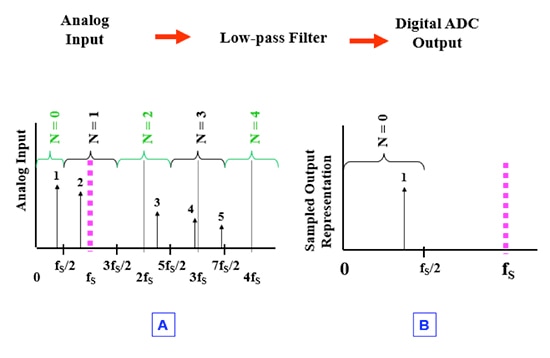
Figure 5: When the signal bandwidth is less than half of the sample rate, the original signal can be reconstructed. If the signal bandwidth is greater than half of the sample rate, the low-pass filter attenuates the signal before the ADC digitization action. (Image source: DigiKey)
A second filtering strategy is to replace the analog filter with a digital filter.
Digital Finite Impulse Response (FIR) filter
Overly confident controller and processor designers believe that they can cure all evils in their digital domain. “Just give me the signal: I will clean it up digitally,” is a common refrain. It’s possible to do a lot in the digital domain, but it’s not a panacea.
A controller or processor designer tends to believe that the FIR is an appropriate digital filter for this purpose. The FIR filter is basically a weighted, averaging filter that over time attenuates high-frequency noise. This filter does not have a feedback loop to provide good stability (Figure 6).
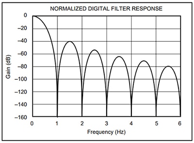
Figure 6: Normalized FIR digital filter response. A FIR filter doesn’t have feedback to provide stability. (Image source: Texas Instruments)
The FIR digital filter computation involves a linear approach (Figure 7).
![]()
Figure 7: Y[N] computation for a FIR digital filter involves a linear approach. (Image source: Microchip Technology)
Where N is the number of taps and a0, a1, … aN-1 are N filter coefficients.
FIR digital filters have a linear phase response. Specifically, the phase is undistorted as it passes through the filter. They are simple to implement as they usually involve the looping of a signal instruction.
The numeric properties of FIR filters are also desirable. Since FIR filters do not have feedback, the implementation uses few bits with fewer non-ideal arithmetic problems.
Compare the two
The digital FIR filter is very attractive. It allows programming on the fly and the ability to create different filter functions, i.e. IIR or even the analog counterpart. This is an easy way to obtain low-cost solutions during the troubleshooting phase.
The digital filter advantages are attractive, except for one fundamental problem. The ADC has already aliased unwanted signals into the signal path. Consequently, the digital filter starts with a contaminated signal.
The analog solution is the way to go. The approach is to eliminate the problems as soon as possible.
Conclusion
Converting analog sensor signals to the digital domain is standard practice for wearable, patient monitoring equipment. The dependence on reliable, repeatable results is critical. An important decision in these designs is to determine whether analog or digital filtering is appropriate.
This article evaluated the difference between analog filters versus digital filters in a data acquisition system. The analog solution uses a low-pass or an anti-aliasing filter prior to the digitization activity. This solution successfully attenuates potential aliased signals from the ADC digital output signal results.
The digital system uses a FIR filter after the signal is digitized. This solution is able to reduce noise using averaging techniques. It is, however, unable to identify the difference between aliased signals and the signals in band. Of the two approaches, the analog filter is the better choice.
References
- Baker, Bonnie C, “Anti-aliasing Analog Filters for Data Acquisition Systems”, AN699, Microchip Technology
- Baker, Bonnie, “Filtering? Before or after?”, EDN, February 20, 2003
- A Baker’s Dozen: Real Analog Solutions for Digital Designers
- Ramu, Anantha, “Implementing FIR and IIR Digital Filters Using PIC18 Microcontrollers”, AN852, Microchip Technology

聲明:各作者及/或論壇參與者於本網站所發表之意見、理念和觀點,概不反映 DigiKey 的意見、理念和觀點,亦非 DigiKey 的正式原則。


