Gate-Level Modeling using Verilog: Hands-on Design Examples – Part 26
2025-09-11 | By DWARAKAN RAMANATHAN
Introduction
While designing digital circuits, it is essential to know the different levels of abstraction. One of the most elementary levels is gate-level modeling, where the behavior of a circuit is defined in terms of elementary logic gates such as AND, OR, XOR, NOT, NAND, and NOR. It is a method that emulates the actual gate-level schematic of hardware and is generally used to model elementary combinational circuits. Though upper levels of abstraction, such as behavioral or RTL modeling, are more suitable for complex designs, gate-level modeling needs to be known in order to acquire a good grasp of digital electronics and hardware description languages such as Verilog.
In this tutorial, we will walk through gate-level modeling examples in Verilog. Examples are the design of a half-adder, a full-adder, and a 2:1 multiplexer. All of them provide a step-by-step description of the design logic, then the Verilog code, testbench, and simulation result explanation.
Half-Adder with Gate-Level Modeling
Half-adder is a basic digital circuit that adds two single-bit binary digits. It has two inputs, A and B, and two outputs—Sum and Carry. An XOR gate is employed to calculate the sum because the output must be 1 if either A or B is 1 but not both. The carry output is calculated by an AND gate because a carry is generated only if both inputs are high.
This basic circuit is where one will usually start learning binary addition in hardware. While it can't handle carry-in from previous stages (something necessary in multi-bit addition), it is employed as the foundation for the full-adder.
Here is the implementation in Verilog using gate-level primitives:
module half_adder (

    input A, B,

    output Sum, Carry

);

    xor (Sum, A, B);

    and (Carry, A, B);

endmodule
The testbench tests all input combinations:
module tb_half_adder;

    reg A, B;

    wire Sum, Carry;

    half_adder uut (.A(A), .B(B), .Sum(Sum), .Carry(Carry));

    initial begin

        $display("A B | Sum Carry");

        A = 0; B = 0; #10;

        $display("%b %b |  %b     %b", A, B, Sum, Carry);

        A = 0; B = 1; #10;

        $display("%b %b |  %b     %b", A, B, Sum, Carry);

        A = 1; B = 0; #10;

        $display("%b %b |  %b     %b", A, B, Sum, Carry);

        A = 1; B = 1; #10;

        $display("%b %b |  %b     %b", A, B, Sum, Carry);

    end

endmodule
Simulation Interpretation
The simulation clearly shows that the sum is high when only one of the inputs is high, and the carry is high when both are high. This verifies the design and shows how even basic gates can be employed to carry out arithmetic operations at the binary level.
Full-Adder using Gate-Level Modeling
Based on the half-adder, a full-adder receives an extra input named carry-in (Cin) to consider carry propagation from the previous stage. This makes it possible to chain several full-adders to implement an entire multi-bit adder. The outputs once more are mixed Sum and Carry-out (Cout).
The logic for a full-adder can be broken down into two phases: First, it determines the carry-in and the sum of A and B (like a half-adder), and then adds the carry-in to get the final sum. The carry-out is calculated based on any two or all three of the inputs being high, through AND and OR gate combinations.
Following is the gate-level implementation of a full-adder:
module full_adder (

    input A, B, Cin,

    output Sum, Cout

);

    wire S1, C1, C2;


    xor (S1, A, B);

    xor (Sum, S1, Cin);

    and (C1, A, B);

    and (C2, S1, Cin);

    or (Cout, C1, C2);

endmodule
The next testbench stimulates all relevant input combinations:
module tb_full_adder;

    reg A, B, Cin;

    wire Sum, Cout;

    full_adder uut (.A(A), .B(B), .Cin(Cin), .Sum(Sum), .Cout(Cout));

    initial begin

        $display("A B Cin | Sum Cout");

        A = 0; B = 0; Cin = 0; #10;

        $display("%b %b  %b  |  %b    %b", A, B, Cin, Sum, Cout);

        A = 0; B = 1; Cin = 1; #10;

        $display("%b %b  %b  |  %b    %b", A, B, Cin, Sum, Cout);

        A = 1; B = 1; Cin = 0; #10;

        $display("%b %b  %b  |  %b    %b", A, B, Cin, Sum, Cout);

        A = 1; B = 1; Cin = 1; #10;

        $display("%b %b  %b  |  %b    %b", A, B, Cin, Sum, Cout);

    end

endmodule
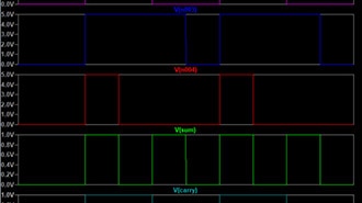
Simulation Interpretation
The simulation confirms the correct functioning of the full-adder. For example, when A = 1, B = 1, and Cin = 1, then the sum is 1 and carry-out is 1, as would be expected. This shows how the more advanced arithmetic operations are built by building on the simple logic gate idea.
2:1 Multiplexer using Gate-Level Modeling
A multiplexer, or briefly MUX, is a combinational circuit that selects one of multiple input signals and directs it to an output line. The 2:1 multiplexer is the most basic and switches in a selection of two inputs with one select line (Sel). If Sel = 0, the output is input A, and if Sel = 1, the output is input B.
The internal logic is to complement the select line and utilize it to select either A or B through the use of AND gates. An OR gate then receives the two resulting signals and produces the end result.
The gate-level Verilog of a 2:1 MUX is as follows:
module mux_2to1 (

    input A, B, Sel,

    output Y

);

    wire nSel, w1, w2;

    not (nSel, Sel);

    and (w1, A, nSel);

    and (w2, B, Sel);

    or  (Y, w1, w2);

endmodule
The testbench here checks every combination of inputs to ensure the selection logic:
module tb_mux_2to1;

    reg A, B, Sel;

    wire Y;

    mux_2to1 uut (.A(A), .B(B), .Sel(Sel), .Y(Y));

    initial begin

        $display("A B Sel | Y");

        A = 0; B = 1; Sel = 0; #10;

        $display("%b %b  %b   | %b", A, B, Sel, Y);

        Sel = 1; #10;

        $display("%b %b  %b   | %b", A, B, Sel, Y);

        A = 1; B = 0; Sel = 0; #10;

        $display("%b %b  %b   | %b", A, B, Sel, Y);

        Sel = 1; #10;

        $display("%b %b  %b   | %b", A, B, Sel, Y);

    end

endmodule
Simulation Interpretation
The simulation output verifies the functionality of the 2:1 MUX. It shows that output Y = A when Sel = 0 and Y = B when Sel = 1, as it would be in the theoretical operation of a multiplexer.
Conclusion
Gate-level modeling is an imperative, schematic-like specification of the behavior of digital logic circuits. Never actually used in large-scale designs today due to verbosity and lack of scalability, it is nevertheless a valuable teaching tool. Being able to build circuits from logic gates enables one to understand what happens inside hardware. Through the example of the half-adder, full-adder, and 2:1 multiplexer, we have shown how simple gates can be used in combination to build interesting digital logic. Through each example, we have demonstrated how the theory's logical constructs translate directly into functional Verilog code. The inclusion of simulation results is the mark of the model's correctness and is also an excellent method of debugging and verification. As you go along with Verilog and digital design education, continue to investigate more advanced-level modules and try to design 4:1 multiplexers, decoders, and arithmetic circuits at the gate level. These exercises will solidify your knowledge in digital logic and ready you for more advanced-level design activity in RTL and system modeling.