How to use LTspice to Determine Photo Sensing Noise Performance During Sensitive Instrument Design
Analog Devices Inc.’s Precision Wide Bandwidth Signal Chains and the LTspice simulator software assist designers with device selection and evaluation. Each signal chain brings insight and application knowledge from ADI by leveraging decades of experience and its analog portfolio.
The Precision Wide Bandwidth Signal Chains give high-precision AC-DC measurement and drive performance. The three block diagrams (current and voltage, current and voltage drive, and light measurements) present individual signal chains, each of which are ready for a variety of application-specific optimizations for signal-to-noise ratio (SNR), DC linearity, settling time performance, closed-loop/measurement latency, and total harmonic distortion (THD) measurements.
The light measurement block diagram matches flow cytometry, spectrometry, chemical analysis, and analytical instrument applications (Figure 1).
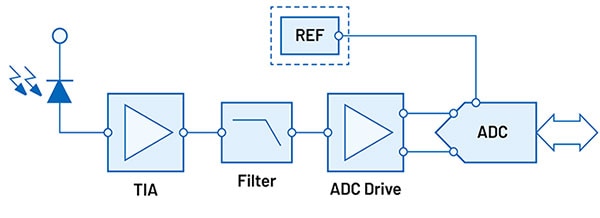 Figure 1: Precision wide-bandwidth, light measurement block diagram for flow cytometry, spectrometry, or other analytical measurement applications. (Image source: Analog Devices)
This solution combines ADI's precision transimpedance amplifiers (TIAs), analog filtering, a voltage reference, and an analog-to-digital converter (ADC).
Light measurement
The TIA must have an extremely low input bias current, low noise, and very wide bandwidth to be suitable for flow cytometry equipment. An appropriate amplifier for this function is Analog Devices’ LTC6268H-10 operational amplifier (op amp) with its ultra-low bias current and 4 gigahertz (GHz) FET input (Figure 2). Its frequency response, when configured as a TIA with a 20 kilohm (kΩ) feedback resistor, is shown (right).
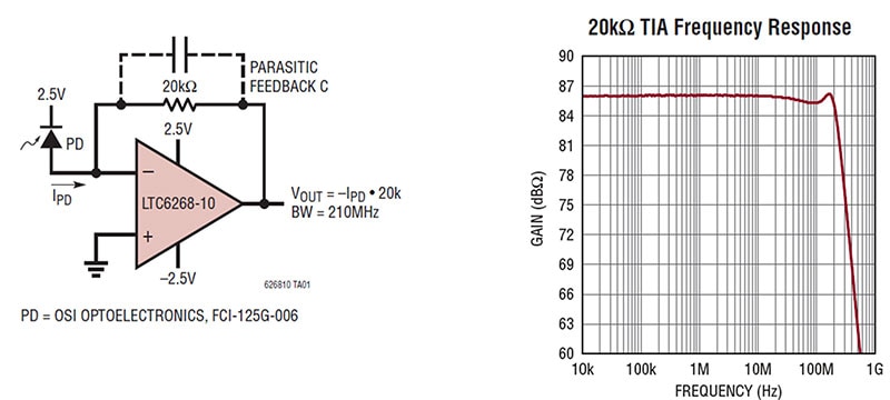 Figure 2: The LTC6268H-10 amplifier’s low input bias current, low noise, and wide bandwidth make it suited for use as a TIA. (Image source: Analog Devices)
In Figure 2, the photodetector (PD) is reverse biased to reduce the parasitic capacitance, and the parasitic feedback capacitance (C) captures the pc board and feedback resistor parasitic capacitance. It is critical that the input bias current of the LTC6268H-10 op amp does not create a significant DC error as it flows through the feedback resistor. The LTC6268H-10 meets this criterion with an extremely low input bias current of ±4 picoamperes (pA). The low noise specification of the LTC6268H-10 is equal to 4 nanovolts per root Hertz (nV/√Hz) at 1 megahertz (MHz).
High-speed flow cytometry requires signal path devices to have a wide bandwidth for a fast slew rate. The LTC6268H-10 bandwidth in this circuit is 210 MHz, which translates to a slew rate of ~1000 volts per microsecond (volts/µs).
Finally, the most critical specification is the noise density, which must be at least three times lower than the ADC noise density. The input noise density of the LTC6268-10 is 4.0 nV/√Hz at 1 MHz. The op amp feedback loop gains this noise. Additionally, an overshadowing 20 kΩ feedback resistor also produces noise directly at the amplifier’s output.
The noise density contribution (VFB) of the 20 kΩ feedback resistor, which at higher frequencies dominates the TIA stage noise contribution, equals:
The responsibility of the third and fourth function in the Figure 2 block diagram is to convert the TIA’s output signal to a digital representation. The combined third, fourth, and reference functions create a data acquisition solution. This solution integrates the filter, driver amplifier, voltage reference, and ADC (Figure 3).
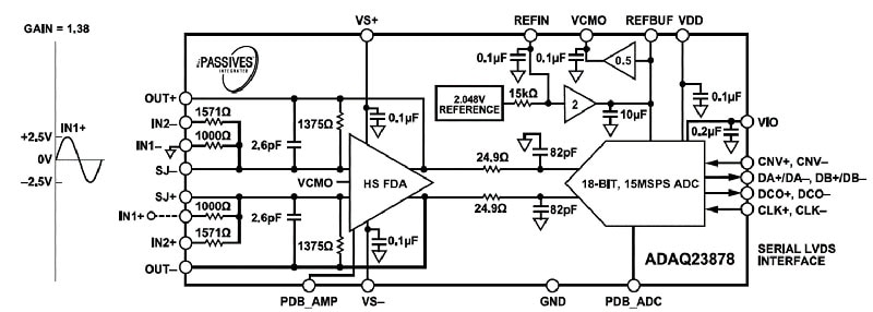 Figure 3: The ADAQ23876 forms a data acquisition solution and is shown as a single-ended input configuration with a gain of 1.38. (Image source: Analog Devices)
In Figure 3, the Analog Devices ADAQ23876 has a 16-bit, 15 mega samples per second (MSPS), successive approximation register (SAR) ADC that provides zero-latency results. The input’s fully differential amplifier (FDA) has an RIN and CIN of 1,407 Ω and 3.3 picofarads (pF), respectively, to create a 1st order low-pass filter.
This system simplifies the circuit designer’s ADC driver and layout challenges by solving the problems internally with the fully integrated device. For this application, the ADAQ23876 configuration caters to a single input signal and implements an internal gain of 1.38, where the typical signal-to-noise ratio (SNR) is 88.8 decibels (dB).
LTspice simulations for circuit analysis
LTspice is high-performance SPICE simulator software that has graphical schematic capture capability. You can probe schematics for simulation results and explore them through LTspice’s built-in waveform viewer.
A circuit’s noise response is often a combination of the individual components in a specific schematic. LTspice’s noise analysis function helps you derive the noise response. To demonstrate, this blog uses a light measurement circuit with a photodiode, TIA, and data acquisition solution models (Figure 4).
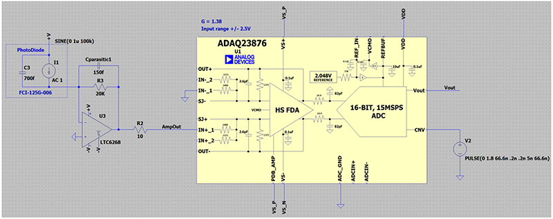 Figure 4: This simulation model uses the LTC6862-10 FET op amp and the ADAQ23876 data acquisition solution to produce noise responses. (Image source: Analog Devices)
In Figure 4, the photodiode model represents an Optoelectronics FCI-125G-006 1.25 gigabit per second (Gbit/s) silicon sensor. The FCI-125G-006 has a 0.66 pF reverse bias parasitic capacitance. The TIA single amplifier of choice, the LTC6268H-10, is stable in closed-loop gains higher than 10 volts/volt (V/V) and has a wide temperature range specification of –40°C to 125°C.
The ADAQ23876 uses system-in-package (SIP) technology which reduces system component count and design complexity by combining multiple common signal processing and conditioning blocks in a single device.
Light measurement noise results
An AC sweep noise simulation is helpful to confirm the ADC resolution of the total circuit. The simulation considers parasitic capacitances and resistances to produce complete noise results across the application’s frequency spectrum. The noise contribution across the entire frequency spectrum of the total application circuit (ADAQ23876 + LTC6268 + FCI-125G-006) is shown as 124.49 microvolts (µV) rms (Figure 5).
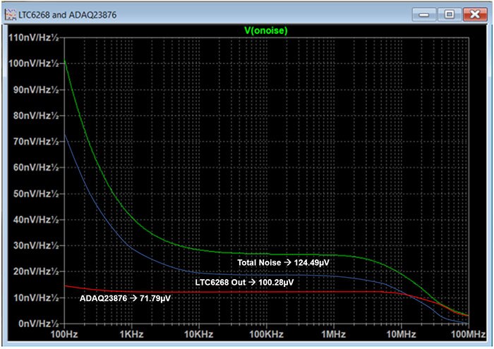 Figure 5: Noise from the ADAQ23876 16-bit ADC and the LTC6268 TIA, shown with the total noise of both devices. (Image source: LTspice, Bonnie Baker)
The total RMS noise contribution across the simulation’s frequency spectrum appears when the user ctrl-left clicks on the curve name at the top of the plot (Figure 6).
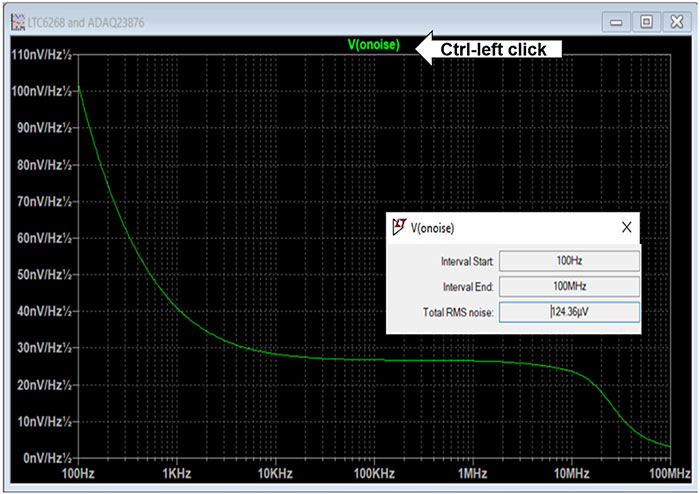 Figure 6: The total noise in the area under the curve depends on the simulation frequency range and the devices’ noise generation value. A simple ctrl-left click provides this rms value. (Image source: LTspice, Bonnie Baker)
The ADAQ23876’s noise production across the entire frequency spectrum equals 71.79 µVRMS. In this plot, the ADC’s 1 MHz voltage spot noise contribution is approximately 12 nV/√Hz. The spot noise, which has a bandwidth of 1 Hz, appears at the bottom left while hovering over the curve.
The LTC6268 TIA noise contribution across the entire frequency spectrum at its output pin is 100.28 µVRMS. The 1 MHz spot noise at the output of the TIA is approximately 18.5 nV/√Hz.
So, the most critical question is, what does this mean in terms of the resolution of the total system?
Conclusion
For photometry-based instrumentation, a photodiode, a TIA such as the LTC6268, and the ADAQ23876 16-bit, 15 MSPS μModule, can be combined to simplify the design of a high-precision, high-speed, complete data acquisition system. Together with the LTspice simulation tool, the combination relieves the designer of tedious noise calculations, high-speed pc board layout, and chip count headaches for precision applications such as flow cytometry.

Have questions or comments? Continue the conversation on TechForum, DigiKey's online community and technical resource.
Visit TechForum


