How JK Flip-Flops Work
With a practical example using the original Digi-Keyer
Introduction
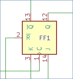
Flip-flops are integrated circuits used to store a single bit of binary data in two stable states. They are widely used for counters, registers, frequency dividers, and, for the example used here, a sequential logic circuit, also known as an astable multivibrator.
There are many types of flip-flops to choose from, with common features such as set and reset inputs, clears, presets, clock inputs, and complimentary logic outputs. They are triggered by a rising or falling edge transition at the clock input. Common types include the SR flip-flop, D flip-flop, or T flip-flop. JK flip-flops are sometimes referred to as “universal” in that they can be configured to emulate many of the other types.
JK Flip-Flop Functionality
When working with flip-flops, it is essential to keep the truth table handy from the device datasheet to determine the output characteristics depending on the multiple input options and clock transitions. Texas Instrument’s CD74HCT73E, for instance, is a typical dual JK flip-flop with common characteristics and an easy-to-read truth table.
There are two basic truths to remember; The Q (bar) or notQ output is always the complement of the Q output and there are only four JK input configurations that determine the output when the clock input transitions from high to low. See Figure 1 for the possible JK configurations. The term toggle means that the present state of the Q and notQ outputs are flipped when J and K are both high and the clock transitions from high to low (condition 4 in the truth table).
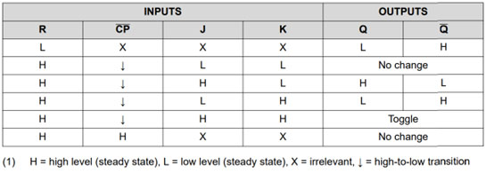 Fig. 1. Typical JK Flip-Flop datasheet truth table.
The basic truths mentioned do not account for the reset (R) input which gives the flip-flop an initial state when the reset is held low. The term “irrelevant” is used in the datasheet with respect to the clock and JK inputs when the reset is low. Changes in these inputs have no effect on the output until the reset is held high and a clock transition is received.
Point to Ponder: When a flip-flop is first powered up, its output is not automatically set to a known state. There is no way to predict which output state will prevail, so the reset input allows an opportunity to initialize the output to a known state after power-up.
Sequential Logic Circuit Example: Morse Character Generator
It takes three DITs to make a DAH
The Digi-Keyer Morse character generator has many components with specific tasks. In order to demonstrate the role flip-flops play, related elements are included with the flip-flops referred to as FF1 and FF2. See Figure 2 for the schematic diagram of the DIT-DAH character-forming section of the Digi-Keyer.
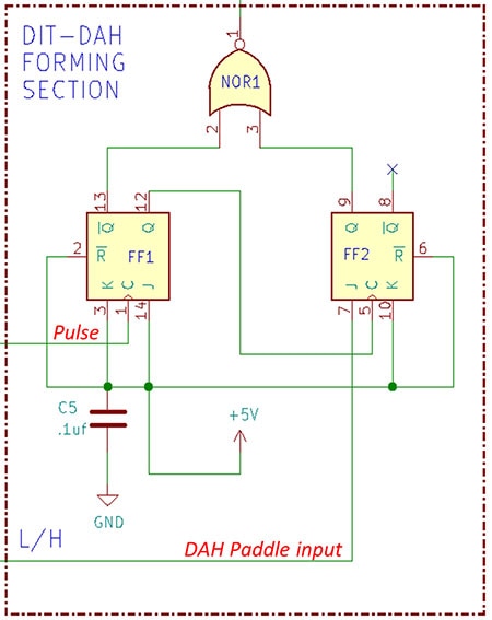 Fig. 2. Digi-Keyer flip-flop character forming circuit
Before diving into creating characters (DITs and DAHs, aka DOTs and DASHES), the function of the NOR1 logic gate must be explained. NOR1 is not only the first stage of the character output circuit. It also enables a timing circuit to deliver regular pulses to FF1 for the duration NOR1 output is low. When NOR1 output is high, the pulses cease at the end of the current timing cycle.
Pressing the DIT paddle switch triggers an initial high-to-low transition pulse from the timing circuit to the C input of FF1. Output pins Q and notQ toggle because the JK inputs are both held high. NotQ triggers NOR1 to output a low signal back to the timing circuit, indicating a DIT is in process. At the completion of the timing function, another pulse is sent to FF1, toggling it back to its normal state. During DIT formation, the Q output of FF1 triggers the C input of FF2, but because the DAH paddle has not been pressed (J input of FF2 is low), the output of FF2 follows condition 3 from the truth table in Figure 1. Figure 3 outlines the resulting sequential logic truth table for generating a single DIT.
 Figure 3. Sequential logic DIT formation truth table.
Pressing the DAH paddle also triggers an initial pulse from the timing circuit that toggles FF1 and sets the J input of FF2 high, causing the FF2 outputs to toggle as well. As the Q output of FF2 also triggers NOR1 output low, the timing pulses continue. The output of NOR1 does not change back to high until FF1 and FF2 have both returned to their normal state, which requires three DIT cycles. Figure 4 outlines the sequential logic truth table for generating a single DAH.
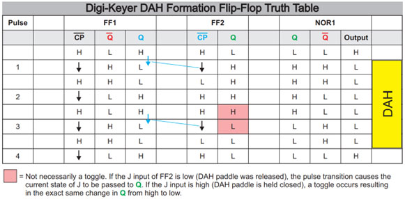 Figure 4. Sequential logic DAH formation truth table.
The length of time that it takes for the flip-flops to return to their normal state depends on the time that passes between high to low transitions. In this example, the low time of one pulse cycle is fixed at 8 ms, but the high time is adjustable from 15 to 150 ms in the timing circuitry. At the slowest setting, DIT characters are about 158 ms in length, and DAHs are about 474 ms. The final high-to-low transition that lands FF1 and FF2 back into their normal state transitions back to high in 8 ms resulting in a fixed space between characters if either or both paddles are held closed (high).
Another point to ponder: At circuit power-up, FF1 and FF2 may end up in random logic states, as mentioned earlier. If any state results in a low at the output of NOR1, the timing circuit will begin sending pulses until FF1 and FF2 reach their normal state. The result is the flip-flops are automatically initialized to their normal state after power-up without using the reset input.
Summary
It can be difficult to follow flip-flop logic step by step, and that is why generating truth tables like Figures 3 and 4 is helpful to visualize the work going on in the background. In this example, multi-step sequential logic was performed without the use of a microcontroller or a fixed, always-running clock. The outputs of the flip-flops are stored data in that it takes a deliberate input change to effect a change in the output. The data is also volatile. When power is removed, the data is lost. The object of the Morse character generator is not to produce data. The flip-flops are used to remember a previous condition to determine the next condition between high to low transitions of the clock pulses.
Resources:
Creating Quasi-Sine from Square Waves
Updating the Original Digi-Keyer
Interested in building the Digi-Keyer and learning how it works? DigiKey provides the full set of plans, bill of materials, programming code, PCB files, and more in this repository:
https://media.digikey.com/pdf/Project%20Repository/Digikeyer.zip

Have questions or comments? Continue the conversation on TechForum, DigiKey's online community and technical resource.
Visit TechForum


