Driving GaN FETs with Controllers Designed for Silicon MOSFETs
Gallium nitride (GaN) devices offer significant performance and efficiency advantages over traditional silicon MOSFET components in power applications. They deliver the higher density, faster switching, and greater energy efficiency needed across a wide range of industries. But for some applications, there are significant design challenges.
From compact USB-C chargers and electronic vehicle on-board chargers to solar energy and data center applications, designers are eager to take advantage of GaN semiconductor technology to deliver smaller, lighter, and cooler products.
Due to the fast switching speeds of GaN components, designers face multiple challenges, including parasitic inductance, the need for more precise gate control, gate leakage current, and reverse conduction voltage drops.
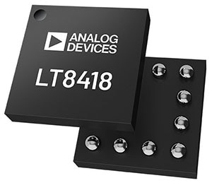
Purpose-built GaN controllers are an ideal choice for designing certain GaN-based applications. For example, Analog Devices, Inc. offers a range of GaN power controllers. Designers can take advantage of simple, dedicated GaN FET drivers such as the LT8418 100 V half-bridge GaN driver with a smart integrated bootstrap switch (Figure 1).
 Figure 1: ADI's purpose-built LT8418 half-bridge GaN driver. (Image source: Analog Devices, Inc.)
This device incorporates split gate drivers to precisely control the slew rates of GaN FETs during turn-on and turn-off, thereby suppressing ringing and enhancing EMI performance. It also utilizes wafer level chip scale packaging (WLCSP) to minimize parasitic inductance.
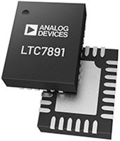
Also available are more complex controllers, such as the LTC7890 and LTC7891 (Figure 2) high-performance, dual step-down, DC/DC switching regulator controllers for GaN FETs.
 Figure 2: ADI's high-performance LTC7891 DC/DC switching regulator controller for GaN FETs. (Image source: Analog Devices, Inc.)
Unlike silicon MOSFET solutions, the LTC7890/LTC7891 devices require no protection diodes or additional external components. Their gate drive voltage can be precisely adjusted from 4 V to 5.5 V to optimize performance and enable the use of other GaN FETs or logic-level MOSFETs.
When a silicon controller is the only option
There are no purpose-built GaN controllers readily available for some critical components, such as 4-switch buck-boost controllers. Designers may be able to adapt existing controllers designed for MOSFETs to drive GaN FETs for enhanced power and efficiency, provided they proceed with caution. Utilizing silicon-targeted controllers for GaN applications requires care in component selection and board-level design, and may involve additional circuitry.
In high-power converters, traditional gate drivers often output voltages above 5 V—typically between 7 V and 10 V, sometimes even higher. This creates a problem when driving GaN FETs, which usually have a maximum gate voltage rating of just 6 V. Exceeding this limit even briefly due to voltage spikes or ringing from stray inductance on the PCB can permanently damage GaN devices.
Designers can avoid these issues by selecting the right controller and paying close attention to PCB layout, especially around the gate and source return paths in order to keep inductance as low as possible, and reduce unwanted voltage overshoot.
Many MOSFET drivers utilize unregulated silicon gate drivers that can drift up above the absolute maximum voltage of GaN FETs. Design considerations include managing the gate drive voltage, regulating the bootstrap supply, and optimizing dead time.
A 4-switch buck-boost device must use a 5 V gate controller to prevent accidental overvoltage of GaN FETs. It's also important to include protective components—such as clamping circuits or gate voltage limiters—to safeguard the gate from accidental overvoltage.
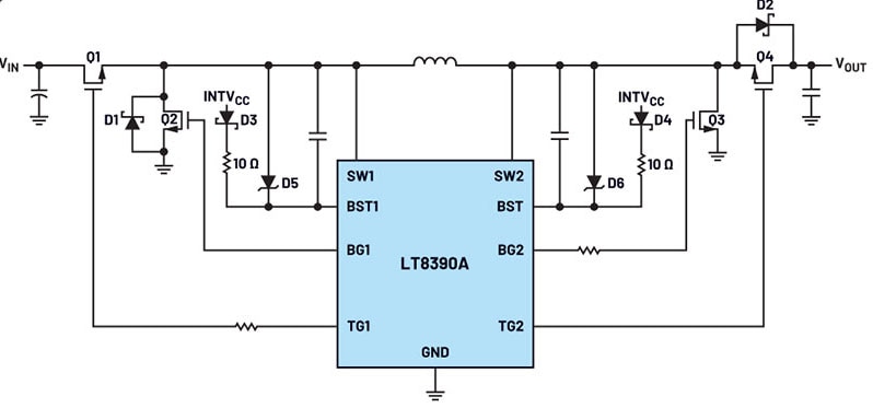
ADI's LT8390A can function as a 5 V gate controller by utilizing 5.1 V Zener diodes placed in parallel with bootstrap capacitors (Figure 3). This clamps the gate voltage at the recommended drive level so it remains within a safe operating range. For additional protection, 10 Ω resistors can be added in series with the bootstraps to reduce any ringing that might be caused by the very fast and high-power switch nodes.
 Figure 3 : This simplified schematic illustrates the LT8390A 4-switch buck-boost controller utilizing 5.1 V Zener diodes (D5 and D6) and 10 Ω resistors for voltage protection in driving GaN FETs. (Image source: Analog Devices, Inc.)
Conclusion
Silicon MOSFET controllers, such as ADI's LT8390A buck-boost controller, can be adapted to drive GaN FETs safely and effectively, enabling designers to create GaN applications even when purpose-built DC-to-DC GaN controllers are unavailable.
For further information, watch the Designing with GaN: Overcoming Challenges in Power webinar.

Have questions or comments? Continue the conversation on TechForum, DigiKey's online community and technical resource.
Visit TechForum


