How to Minimize Parasitics in Switching Power Supplies
Contributed By DigiKey's North American Editors
2024-01-31
Switch mode (switching) power supplies are popular for their efficiency and flexibility. They also bring challenges as they extend their reach into new applications. Most notably, their high-frequency switching can induce electromagnetic interference (EMI) in the rest of the system. Moreover, the same factors that can lead to EMI also reduce efficiency, undermining one of the key benefits of switching power supplies.
To avoid these issues, designers must take special care when configuring the “hot loop,” the portion of the power supply circuit where rapid switching occurs. Minimizing the hot loop’s parasitic losses due to equivalent series resistance (ESR) and equivalent series inductance (ESL) is essential. This can be accomplished by choosing highly integrated power supply components and a careful printed circuit board (pc board) layout.
This article introduces hot loops and the sources of parasitic loss, including coupling capacitors, power field-effect transistors (FETs), and pc board vias. It then shows an example of a highly integrated power converter from Analog Devices and presents various pc board layouts and their effects on parasitic parameters. It concludes with practical tips for ESR and ESL reduction.
Fundamentals of switching power supply hot loops
Any power supply design that involves rapidly switching currents, such as boost, buck-boost, and flyback converters, will have hot loops with currents switching at high frequencies. This concept is illustrated through a simplified buck converter, also known as a step-down converter (Figure 1). The loop on the left (red) contains all the switching elements; the high-frequency currents generated by the circuit are contained within, forming the hot loop.
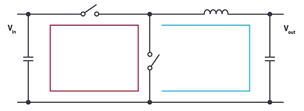 Figure 1: A simplified buck converter illustrates the principle of a hot loop, highlighted in red. (Image source: Analog Devices)
The “hot” aspect comes from the significant energy conversion and switching activities occurring in this area of the circuit, often accompanied by heat generation. The proper layout and design of these hot loops are critical to minimize EMI and ensure efficient power supply operation.
The more realistic circuit in Figure 2 shows a DC-DC synchronous buck converter. For this hot loop, the physical components (labeled in black) are the input capacitor (CIN) and the switching metal-oxide-semiconductor FETs (MOSFETs), M1 and M2.
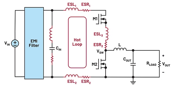 Figure 2: Real-world hot loops inevitably include parasitic parameters, shown in red. (Image source: Analog Devices)
The parasitic parameters within the hot loop are labeled in red. The ESL is typically in the nanohenry (nH) range, while the ESR is in the milliohm (mΩ) range. The high-frequency switching causes ringing within the ESLs, resulting in EMI. The energy stored in the ESLs is then dissipated by the ESRs, leading to power loss.
Minimizing parasitic parameters with integrated components
These parasitic impedances (ESRs, ESLs) occur within the components and along the hot loop pc board traces. To minimize these parameters, designers must carefully choose components and optimize the pc board layout.
One way to achieve both goals is to use integrated components. These eliminate the pc board traces required to connect discrete components while reducing the hot loop's overall area. Both contribute to reducing parasitic impedance.
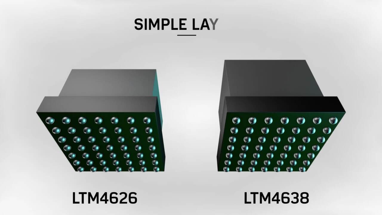
An excellent example of a highly integrated component is the LTM4638 step-down µModule regulator from Analog Devices. As illustrated in Figure 3, this 15 ampere (A) switching regulator integrates the switching controller, power FETs, inductor, and support components, all in a tiny package measuring 6.25 × 6.25 × 5.02 millimeters (mm).
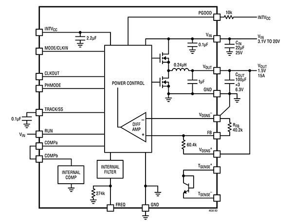 Figure 3: The LTM4638 µModule regulator integrates many of the components needed for a buck converter. (Image source: Analog Devices)
The LTM4638 incorporates several other features that reduce parasitic losses. These include:
- Fast transient response: This enables the regulator to quickly adjust the output voltage in response to changes in the load or input, minimizing the duration and impact of parasitic losses by quickly transitioning through sub-optimal operating states.
- Discontinuous mode operation: This allows the inductor current to drop to zero before the next switching cycle starts. Typically used under light load conditions, this mode reduces switching and core losses in the inductor by de-energizing it for part of the cycle.
- Output voltage tracking: This enables the converter output to follow a reference input voltage. By precisely controlling the ramp up and ramp down of the output voltage, this feature reduces the likelihood of overshoots or undershoots that can exacerbate parasitic losses.
Minimizing parasitic parameters with component placement
Constructing a synchronous buck converter with the LTM4638 requires adding bulk input and output capacitors, CIN and COUT, respectively. The positioning of these capacitors can have a significant impact on parasitic parameters.
Analog Devices' experiments with the DC2665A-B evaluation board for the LTM4638 illustrate the impact of CIN positioning. The DC2665B-B has since replaced this board, but the same principles apply. Figures 4 through 6 illustrate three different layouts for CIN and the corresponding hot loops. Vertical Hot Loops 1 (Figure 4) and 2 (Figure 5) place CIN on the bottom layer, directly below the regulator or to the side, respectively. The Horizontal Hot Loop (Figure 6) places the capacitor on the top layer.
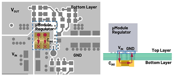 Figure 4: Vertical Hot Loop 1 bottom and side view. CIN is directly beneath the regulator, connected through vias. (Image source: Analog Devices)
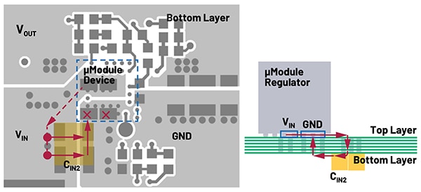 Figure 5: Vertical Hot Loop 2 bottom and side view. CIN is below but beside the regulator, requiring pc board traces and vias. (Image source: Analog Devices)
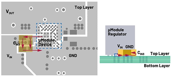 Figure 6: Horizontal Hot Loop top and side views. CIN is on the top layer, connecting to the regulator through traces. (Image source: Analog Devices)
Vertical Hot Loop 1 has the shortest path and avoids using pc board traces. Thus, it would be expected to have the lowest parasitic parameters. Analyzing each hot loop with FastHenry at 600 kHz and 200 megahertz (MHz) reveals that this is the case (Figure 7).
|
Figure 7: As expected, the shortest path had the lowest parasitic impedance. (Image source: Analog Devices, modified by author)
Although these parasitic parameters cannot be directly measured, their effects can be predicted and tested. Specifically, a lower ESR should lead to higher efficiency, while a lower ESL should result in lower ripple. Experimental verification confirmed these predictions, with Vertical Hot Loop 1 demonstrating better performance on both metrics (Figure 8).
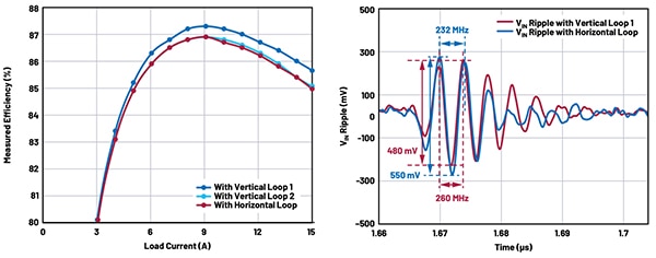 Figure 8: Experimental results confirm that Vertical Hot Loop 1 achieves better efficiency and ripple. (Image source: Analog Devices)
Minimizing parasitic parameters for discrete components
Although integrated devices offer many advantages, some switching power supplies require discrete components. For example, a high-power application might exceed the capabilities of integrated devices. In such cases, the placement and package size of the discrete power FETs can significantly impact hot loop ESRs and ESLs. These impacts can be seen by testing two evaluation boards, both featuring high-efficiency, 4-switch synchronous buck-boost controllers, as illustrated in Figure 9:
- The DC2825A evaluation board is based on the LT8390 buck-boost regulator. Its MOSFETs are placed in parallel, i.e., in the same orientation.
- The DC2626A evaluation board is based on the LT8392 buck-boost regulator. It has two pairs of MOSFETs placed at 90˚ angles.
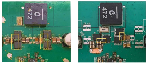 Figure 9: The DC2825A (left) places its MOSFETs in parallel, while the DC2626A (right) places them at 90˚ angles. (Image source: Analog Devices)
The two boards were tested using identical MOSFETs and capacitors in a 36 to 12 volt step-down operation at 10 A and 300 kilohertz (kHz). The results showed that the 90˚ placement had a lower voltage ripple and a higher resonant frequency, indicating a smaller pc board ESL due to a shorter hot loop path (Figure 10).
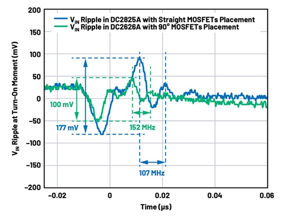 Figure 10: The DC2626A, with its 90˚ MOSFET layout, exhibits lower ripple and higher resonant frequency. (Image source: Analog Devices)
Other layout considerations
Via placements in the hot loop also impact the loop ESR and ESL. In general, adding more vias reduces the pc board parasitic impedance. However, the reduction is not linearly proportional to the number of vias. Vias closer to the terminal pads significantly reduce ESR and ESL. Therefore, multiple vias should be placed close to the pads of the critical components (CIN and the µModule or MOSFETs) to minimize hot loop impedance.
There are many other ways to impact electrical and thermal performance positively. To optimize the hot loop, best practices include:
- Use large pc board copper areas for high current paths, including VIN, VOUT, and ground to minimize pc board conduction loss and thermal stress.
- Place a dedicated power ground layer underneath the unit.
- Use multiple vias for interconnection between the top and other power layers to minimize conduction loss and reduce module thermal stress.
- Do not put vias directly on the pad unless they are capped or plated over.
- Use a separated signal ground copper area for components connected to signal pins, joining the signal ground to the main ground pin underneath the unit.
- Bring out test points on the signal pins for monitoring.
- Keep separation between the clock signal and frequency input traces to minimize the possibility of noise due to crosstalk.
Conclusion
The parasitic parameters within the hot loop heavily influence the performance of a switching power supply. Minimizing these parameters is crucial for achieving high efficiency and low EMI.
One of the simplest ways to reach these goals is by using integrated regulator modules. However, switching power supplies typically require the use of bulk components such as capacitors, so it is essential to understand the implications of hot loop layouts.

Disclaimer: The opinions, beliefs, and viewpoints expressed by the various authors and/or forum participants on this website do not necessarily reflect the opinions, beliefs, and viewpoints of DigiKey or official policies of DigiKey.


