Why and How to Use Digital Filters for High-Resolution, High-Speed, Analog-to-Digital Conversions
2021-03-17
It’s still an analog world, yet digital electronics are pervasive, and for good reason. While digital does solve multiple problems with algorithmic approaches, even the best digital algorithms have shortcomings dealing with real-world entities that exist in the analog domain. This is especially true in applications demanding high-speed and high-resolution data acquisition such as instrumentation, motor control, and data acquisition systems.
The problem for designers looking to capture and process such real-world signals is the need to enter the digital domain as soon as possible without compromising that signal information. The solution comes from a simple averaging algorithm (to reduce noise) with a front-end analog low-pass filter (LPF). With these techniques, a suitable device can provide high-resolution, high-speed conversion with onboard analog and digital filtering.
This article briefly discusses the issues associated with achieving high-resolution, high-speed conversions with a successive approximation register (SAR) analog-to-digital converter (ADC) using an analog LPF and an averaging digital filter, and why this filter combination is a good option for most applications. It then introduces the Analog Devices AD7606C-18 eight-channel SAR ADC and shows how to take advantage of its 1 megasample/s (MSPS) conversion rate, simultaneous sampling converter array, and flexible digital filter functions.
To show how to achieve the best overall performance, this article combines the AD7606C-18 with the ADR4525 ultralow noise, high accuracy voltage reference, also from Analog Devices, to enhance the needed SAR accuracy for 18-bit conversions.
Analog versus digital filters
If an analog engineer and digital engineer discuss filters, the digital engineer may dismiss analog. This would be a mistake. The filtering standard with any analog-to-digital (A/D) conversion is to have the analog LPF before the digital filter (Figure 1).
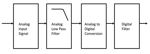 Figure 1: A block diagram of an analog-to-digital signal chain with the analog filter before the digital filter. (Image source: DigiKey)
After the analog LPF attenuates higher frequencies above the bandwidth of interest, the ADC converts the signal into a digital word. Following this accomplishment, the digital filter can operate on the signal within the bandwidth of interest.
Analog filters in data acquisition environments
The importance of the analog LPF comes to light at the ADC’s output. Any signal that passes through the ADC has a magnitude and frequency associated with it. At the ADC’s output, the magnitude of the signal reliably remains the same if the signal frequency is below the ADC’s input bandwidth. Although the A/D conversion preserves the signal magnitude, the same is not true for the signal’s frequencies. One can observe a change in the frequencies above ½ of the ADC’s sampling frequency, fS, also known as the Nyquist sampling rate (Figure 2).
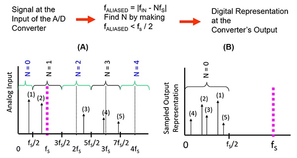 Figure 2: In graph (A), the fast Fourier transform (FFT) representation of an input signal has five frequency components. After an A/D conversion, the FFT representation in graph (B) shows all five signals occurring below half of the ADC’s sampling frequency (fS). (Image source: DigiKey)
In Figure 2, both FFT plots use a logarithmic frequency on the x-axis and a linear voltage or magnitude on the y-axis. In graph (A), the analog signal FFT representation shows an ADC’s input signal with multiple signals or noise above half the ADC sampling frequency, or fS/2.
Comparing these two graphs, it is helpful to follow the five FFT signals. After an ADC conversion, the original signal’s magnitudes remain the same, but the frequencies above half of the sampling frequency in (A) are “flipped” back below fS/2 in (B). This phenomenon is known as signal aliasing. To accurately acquire the signal, the ADC’s sampling rate fS must be greater than two times fMAX, where fMAX is equal to the signal’s usable bandwidth, per the Shannon-Nyquist sampling theorem.
One can see how ADCs permanently implant unwanted noise and signals into the digital output signal. This change makes it impossible to tell the difference between in-band signals and out-of-band signals at the converter’s output.
One might expect that there is a pathway back and forth between these two FFT representations. Once this transformation has occurred, however, there is no going back and undoing it. Unfortunately, mathematics does not support this type of back and forth transition.
Back to the analog/digital debate: a digital filter is undoubtedly capable of applying averaging, finite impulse response (FIR) or infinite impulse response (IIR) filtering, and thereby reduce system noise. However, every digital filter requires a significant amount of oversampling (the process of sampling a signal at a sampling frequency significantly higher than final output data rate) which takes time, power, and reduces the ADC’s sampling speed. The digital filter and converter function never overcome the aliased signal phenomena. It is best to simply reduce the higher frequency noise from the onset—even with a rudimentary analog first-order LPF.
Averaging digital filters
SAR ADCs improve their DC noise measurement with an averaging digital filter. The averaging digital filter acquires multiple conversions with a consistent time scale to increase the number of bits. ADC users use averaging algorithms with their controller, processor, or an on-chip averaging engine that captures several converter samples. The averaging process “smooths” the conversion group and improves the effective resolution by system noise reduction.
Implementing the converted data smoothing involves multiple signal acquisitions at a constant sample rate and averaging a predetermined sample number. The process of averaging is well known. The summation of the ADC results (successive samples, x) divided by the number of samples (N) produces an average value (Equation 1).
![]() Equation 1
Equation 1
This process reduces the output data rate by a factor of N but increases the system’s settling time.
The standard deviation of the averaged noisy samples (σavg) is the standard deviation of the original signal (σsig) divided by the square root of N (Equation 2).
![]() Equation 2
Equation 2
The successive samples, including uncorrelated noise, will result in more noise reduction in a constant signal average. Each consecutive sample averaged causes the signal-to-noise ratio (SNR) to improve if the signal is DC and the noise component is random.
The SNR improvement is proportional to the square root of the number of averaged samples. An average of four DC signal samples (41) will increase the converter’s effective resolution by one with a 6 decibel (dB) increase in the SNR. A 16, or 42, sample average increases the effective resolution by two and the SNR by 12 dB. With this logic, a group size of 4N will increase the number of effective bits from a conversion by N, bringing the system noise to zero and the SNR value to infinity.
The Allan variance
An SNR value equaling infinity is absurd, of course. In the real world, the acquisition of the needed number of samples takes time, during which the system may change in terms of degrees of drift.
The Allan variance, known as two-sample variance, measures the frequency stability in clocks, oscillators, ADCs, and amplifiers by showing the change in noise as the number of samples used in the averaging of a signal is increased. The Allan variance statistical analysis tool determines the maximum number of required samples that will be optimal for a particular system, thereby estimating stability by pointing out frequency drift or temperature effects.
For instance, data in a system from an ADC over time can exhibit shifts as shown in Figure 3.
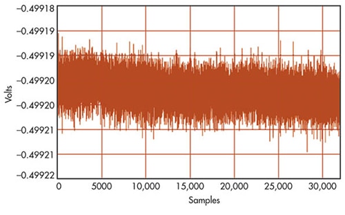 Figure 3: The 30,000 ADC output data points captured over nine minutes show a slight drift in the data over that period, causing a degradation in the Allan variance calculation. (Image source: Electronic Design)
The variance algorithm takes multiple batches of longer and longer averages and assesses each batch’s resulting noise (Figure 4).
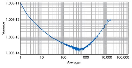 Figure 4: Applied Allan variance calculation for the data points in Figure 3. At the 500 point average, this particular ADC system acquires 4.48 bits or a 27 dB SNR increase. (Image source: Electronic Design)
Figure 4 demonstrates that the minimum variance of this particular system’s data points occurs at approximately 500 ADC output averages—the optimum number of sample averages for reduction of noise. At the 500 point average, this ADC system acquires 4.48 bits or a 27 dB SNR increase. Before and beyond the 500th average point, the results worsen in Figure 4, as data drift becomes a larger factor. Variables that impact the Allan variance calculations can be time, signal stability, drift, power supply variations, and product aging. If a digital averaging filter is in use, it is prudent to evaluate the overall system with the Allan variance tool.
Real-world solution
SAR converters can offer programmable-gain amplifier (PGA) and digital filter functions to enhance the effective resolution and least significant bit (LSB) voltage. For instance, Analog Devices’ AD7606C-18 is an 18 bit, 1 MSPS simultaneous sampling, A/D data acquisition system (DAS) with eight channels, each containing analog input clamp protection, a PGA, an LPF, and an 18-bit SAR ADC.
The device also has analog input buffers with a 1 megaohm (MW) input impedance and programmable true bipolar differential, bipolar single-ended, and unipolar single-ended input voltage configurations. The AD7606C-18 allows the connection of eight different independent input sensors or signal channels.
The AD7606C-18’s digital filter has an oversampling mode that averages repetitive samples from 1 to 256 (44). Per the Allan variance tool, this oversampling feature improves the noise performance at the converter’s digital output. The ADR4525 low noise, 2.5 volt precision voltage reference complements the AD7606C-18 DAS system with a 1 part per million per degree Celsius (ppm/°C) maximum temperature coefficient and 1 microvolt (mV) peak-to-peak typical output noise (Figure 5).
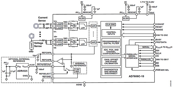 Figure 5: The AD7606C-18 SAR-ADC with the ADR4525 2.5 volt precision voltage reference. The inductors with first-order LPFs on the V1 through V8 input channels simultaneously sample all eight channels. (Image source: Analog Devices)
As Figure 5 shows, this type of high input impedance SAR array can interface directly with sensors minus the typical external driving amplifiers. An external sensor gain stage can also be unnecessary. Concurrently, the SAR converter has an internal PGA and LPF stage that provides signal processing, followed by an averaging digital filter to reduce noise further by providing higher effective resolutions. Such a DAS can offer a 17.1 bit effective resolution with a conversion speed of 3.9 kilosamples per second (ksps). On the other end of the conversion speed spectrum, this device offers a 15 bit effective resolution with a conversion speed of 1 MSPS.
The fastest conversion speed of the AD7606C-18 is 1 MSPS with oversampling equaling one. If the converter’s channel oversampling is two, or averages a channel’s samples twice, the conversion speed is half of the maximum conversion speed at 500 ksps. For oversampling equaling four, or 41 as the number of samples averaged, the conversion speed of that channel is 250 ksps, and so on. For each of the eight channels, the system with an oversampling value of 256 provides a ±10 volt single-ended range, 17.1 bit effective resolution (105 dB SNR), with a conversion speed of 3.9 ksps (Table 1).
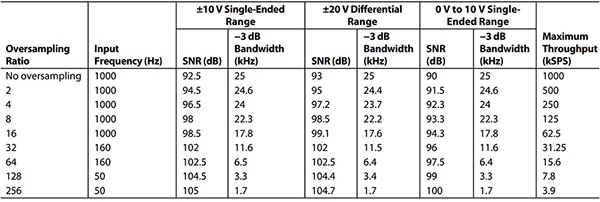 Table 1: Oversampling performance, low bandwidth mode of the AD7606C-18. (Table source: Analog Devices)
The SNR-to-effective-resolution (effective number of bits, or ENOB) conversion formula is shown in Equation 3.
![]() Equation 3
Equation 3
On the other end of the conversion speed spectrum, with an oversampling factor of 1, this device provides 15 bit effective resolution (92.5 dB SNR) with a conversion speed of 1 MSPS (Table 1).
There are further enhancements that the AD7606C-18 offers. Since there are eight separate SAR ADCs on-chip, all eight channels have a simultaneous sampling function. With this function, it is possible to implement the digital filter to achieve high resolution or high speed concurrently on all channels. Additionally, all channels have calibration and diagnostic capability.
For example, the AD7606C-18’s system phase calibration senses the mismatch of the discrete input filter. This valuable feature identifies any mismatch on the discrete components or in the sensor used that can cause phase mismatch between simultaneously sampled channels. The device’s software mode compensates the phase mismatch on a per-channel basis by delaying an individual channel’s sampling instant.
The system gain calibration senses the resistor mismatches of the discrete input filter. This capability helps to overcome external resistor mismatches. The software mode compensates gain error on a per-channel basis by writing the series resistor value used on the corresponding register.
The system offset calibration accommodates the input signal offsets during the calibration activity. The software can adjust each channel’s external sensor’s offset or any external resistor pair mismatch offset.
For a specific application, the EVAL-AD7606SDZ board for the AD7606 has software to assist in device evaluations with device programming, as well as waveform, histogram, and FFT capture (Figure 6).
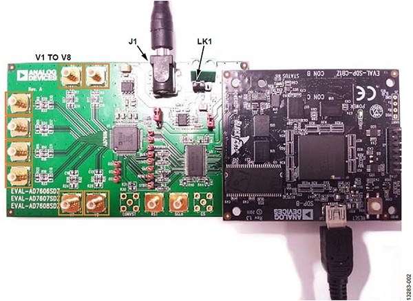 Figure 6: The AD7606 evaluation board (left) connected to the system demonstration platform (SDP) board (right), which allows the evaluation board to be controlled through the USB port of a PC. (Image source: Analog Devices)
The evaluation board’s software allows the user to configure each channel’s oversampling value, input range, number of samples, and active channel selection. Additionally, this software also makes it possible to save and open test data files.
Conclusion
Despite a shift to digital, it’s still an analog world and designers need analog-centric electronics to solve high-resolution, high-speed conversion problems. As shown, the simple combination of an analog LPF and digital averaging filter—implemented with the appropriate number of averaged samples—greatly enhances the performance of a 1 MSPS SAR converter.
Disclaimer: The opinions, beliefs, and viewpoints expressed by the various authors and/or forum participants on this website do not necessarily reflect the opinions, beliefs, and viewpoints of DigiKey or official policies of DigiKey.


