Test Switched-Mode Power Supplies Faster Using Dedicated Oscilloscopes and Software
Contributed By DigiKey's North American Editors
2017-05-17
To meet efficiency and form factor requirements, switched-mode power supply manufacturers are incorporating new semiconductors and circuit topologies, while also adhering to higher standards of power integrity. As a result, designers must make more complex measurements of switched-mode waveforms, which increases test time and adds cost.
In an effort to reduce test time, test equipment makers have developed hardware and software that work together to automate many of the functions and complex analysis. A good example of this combination is the Teledyne LeCroy HDO4104 oscilloscope with Power Analyzer software. This article will describe how the two can be used to perform critical analyses to shorten power supply development and test.
Efficiency, weight, and size drive innovative design and test approaches
Switched-mode power conversion, be it in power supplies, inverters, DC-DC converters, or motor controllers, offers the advantages of higher power efficiency and smaller size and weight for a given power level. However, these features have a cost in the form of greater complexity and higher component stress.
To address this, manufacturers are turning to new semiconductor types, a wider range of circuit topologies, and higher standards of power integrity. However, these demand detailed analysis of key characteristics such as:
- Power losses
- Safe operating area (SOA)
- Control-loop margins
- Line power integrity
- Power supply performance
These are the types of analyses that increase the levels of required development and test engineering expertise, which in turn add test time and increase final product cost. They are also the types of analyses the HDO4104 and Power Analyzer software were designed to simplify.
The HDO4104 is a high resolution, 12-bit oscilloscope with touchscreen. The power analyzer software makes use of the scope’s touchscreen to create a dedicated user interface. With automatic measurements, the combination of hardware and software simplifies critical power switching device measurements, control loop modulation analysis, and line power harmonic testing. The company also offers accessories including differential amplifiers, differential probes, current probes, and deskew fixtures.
Device analysis using the HDO4104
Switched-mode power supplies commonly control the output voltage by using pulse width modulation (PWM) of the power devices. The voltage and current in the supply power device switch between their ON and OFF states. The phasing of the waveforms is such that when the voltage is high, the current is low. As a result, very little power is dissipated by the switching device: power is dissipated only during the transitions between the ON and OFF states (Figure 1).
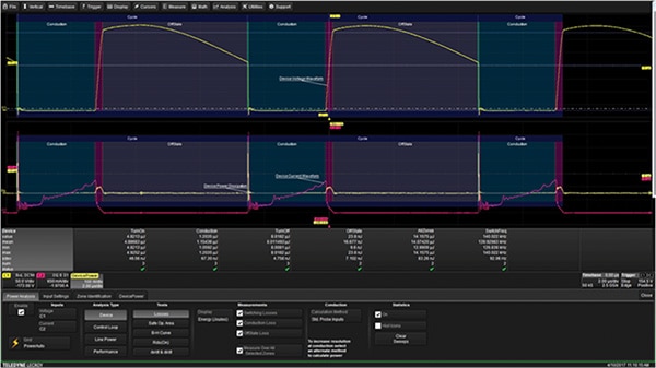
Figure 1: During the analysis of a switched-mode power supply using the Teledyne LeCroy HDO4104 with Power Analysis, both the voltage across the power transistor, as well as the current through it, are acquired. From these, the power dissipation is computed and displayed. (Image source: DigiKey)
The figure shows a basic device measurement using the power analysis software. The dialog box at the bottom of the figure shows the setup and is organized such that it is operated from left to right. After first enabling the power analysis operation, the user selects the signal sources. In this case, a Teledyne LeCroy DA1855A differential amplifier and a CP030 current probe were used.
The next step is to select one of the four types of analysis. This is followed by the selection of the specific test related to each analysis type. In Figure 1, the selected analysis type is Device and the tests being shown are device losses. The voltage across (upper, yellow trace) and the current through (lower, red trace) the switching device are used to calculate its power dissipation (lower, yellow trace). The display uses colored overlays to automatically show the times when the device is conducting and when it is turned off.
The table below the graphic display lists the device power dissipation for each phase of the operating cycle. The phases are turn on, conduction, turn off, and off state. Losses can be measured as power or energy loss. Energy loss is shown in Joules. Note that this computation is automatic, based upon the acquired waveforms.
Other tabs on the dialog box are used for the input setup, zone identification, and scaling of the power trace. The input setup is important because it is used to identify the voltage and current probes used with the oscilloscope. The most important feature is the control to deskew these probes so that current and voltage measurements are time synchronous.
User Tip: Deskewing is critical to making good power loss measurements. A good indication of correct deskew settings is that the Off State power loss is near zero. In the example shown, the deskew setting is correct, and the off-state power loss is less than one thousandth of the other loss readings.
Plotting the SOA to confirm operating margins
Each switching device has maximum limits for voltage, current and power, as specified by the device manufacturer and displayed on its technical data sheet. Reliability of the power supply is dependent on not exceeding these limits. Safe Operating Area (SOA) plots help confirm operating margins during all aspects of circuit operation. SOA is an X-Y plot of the voltage across a device and the current through it. The current and voltage waveforms for a power FET in a switched-mode power supply, along with the SOA plot taken over 30 power cycles, is shown (Figure 2).
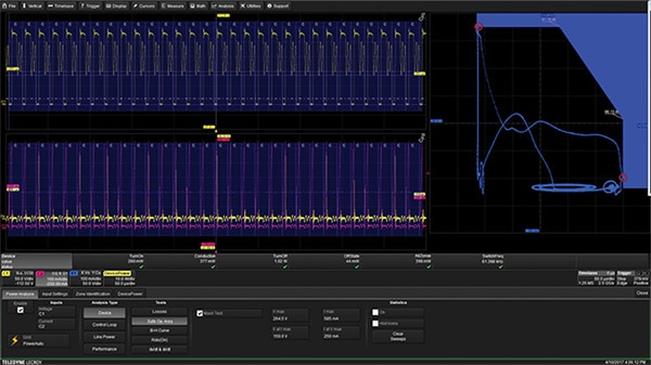
Figure 2: The Safe Operating Area plot on the right records the trajectory of the current and voltage pairs over multiple power cycles. The maximum voltage point is at the extreme right of the plot. The maximum current is at the top. Both points intersect the test mask and are marked by red highlights. (Image source: DigiKey)
The SOA plot shows the current on the vertical axis and voltage on the horizontal axis. The sample-by-sample product of those two signals is the instantaneous power dissipated by the device. The lower left corner of the SOA plot is the point where both the current and voltage are zero. The point to the extreme right is the maximum voltage the device experiences. The vertical extreme is the maximum current through the device.
The SOA plot is displayed within a test mask, which is described by four points:
- Maximum voltage
- Maximum current
- Current at maximum voltage
- Voltages at maximum current
These points are entered by the user in the dialog box shown in Figure 2, using the manufacturer specified limits for the device being tested. If the SOA plot intersects the test mask, a red circle highlights that sample. This circle indicates that the test limit of the mask has been exceeded. Examples of two such intersections are shown.
Where the SOA plot is mainly concerned with voltage, current, and power maxima, the measurement of FET dynamic ON resistance (Rds(ON)) involves a detailed measurement of the FET saturation voltage and channel current (Figure 3).
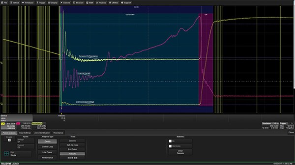
Figure 3: The dynamic ON resistance of a FET (Rds(ON)) is calculated based upon the ratio of the saturation voltage to the channel current. (Image source: DigiKey)
This measurement can be difficult to make because the scope is looking at a signal level of only a few volts in the presence of a voltage swing of several hundred volts.
A good differential amplifier, such as Teledyne LeCroy's DA1855A, makes such measurements easier and more accurate by acting as a signal conditioning preamplifier. The DA1855A also features fast overdrive recovery. Using a ÷ 100 probe, the DA1855A settles to within 100 mV referred to input from a 400 volt input signal within 100 ns. This allows the MOSFET's signal to be overdriven off the screen while the vertical scale is used to zoom in on the section of interest. Note that attempting this technique on the oscilloscope input directly will often saturate the instrument's front-end amplifier.
The DA1855A’s fast overdrive recovery also lets the user overdrive the signal without worrying about errors when the trace comes back on screen. As a result, very good detail can be achieved on saturation voltage.
Calculating the channel ON resistance requires acquiring the FET saturation voltage and its corresponding channel current. From here the simple application of Ohm’s law produces the resistance value. The Power Analyzer software isolates the FET voltage during the conduction phase of the power cycle and performs the measurement automatically using the correct voltage and current segments. In the example in Figure 3, the result is 1.1 Ω.
Other device-related tests available are the time rate of change of the voltage and current waveforms (dV/dt and dI/dt). This shows the rate of change of the voltage and current at device turn on and turn off.
Device testing also extends to magnetic measurements in the form of a B-H curve analysis. The B-H curve displays the saturation status of magnetic devices like transformers. It is a plot of magnetic flux density (B) versus magnetic field strength (H).
The device analysis toolkit offers a complete view of the critical issues related to the switching devices and key magnetic components. The next measurement challenge is the switch mode control loop.
Control loop analysis
Switched-mode power converters use feedback to control the output voltage or current and keep the output within acceptable limits. Most switched-mode power supplies use PWM in their control loops. The width of the drive pulse is increased to raise the output voltage or lowered to reduce it. Control loop analysis allows close study of this feedback loop, especially during transient conditions. However, analysis of the loop dynamics requires the ability to demodulate the PWM signals.
The Power Analyzer software includes easy-to-use modulation analysis capabilities that measure the width or duty cycle of each pulse and creates a plot of pulse width or duty cycle versus time. This is a convenient tool for intuitively viewing the time-domain response of the entire control loop, including any time constants added by the pulse-width modulator in the control IC. To illustrate the concept, the effect of a step load change on the pulse width of the gate drive signal to the switching FET is shown (Figure 4).
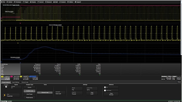
Figure 4: The response of the control loop to a step change in load is displayed for the gate drive signal. The control loop analysis plot shows the controller response as it manages the change by altering the duty cycle of the gate drive signal. (Image source: DigiKey)
The load current, trace C2 (red) in the upper grid, has a positive step of 500 mA. The gate drive signal is acquired on trace C1 (yellow) and shows the controller response to the load change in the width of the gate drive pulses. The control analysis trace (blue) shows the dynamics of the control loop response to the step change in load current.
The trace in the center grid is a horizontal zoom of the gate drive signal. The zoomed section is highlighted on the gate drive trace to show its location relative to the load change. The user can see the variation in pulse width quite clearly on the zoom trace.
The measurement parameters table below the trace grids show the last, mean, maximum, minimum and standard deviation of the parameters frequency period, width and duty cycle for the gate drive signal. This provides a quantitative description of the change in the gate drive signal before and after the load change. In this example the key values are the minimum, maximum and last values of the duty cycle. The minimum value is the initial duty cycle prior to the load change. At this point, the duty cycle is at its minimum value of 4.8%. At the peak of the control analysis plot, the duty cycle is 15.5%, read by the maximum value of the duty cycle parameter. The settled value of the duty cycle in the acquired history is the value of the duty cycle. This is the last duty cycle value read in the waveform, which has the value of 8.9%.
The control loop analysis type can also be used to track PWM regulator response during power startup or shutdown. The startup of a power supply is illustrated in Figure 5. The traces, from top to bottom are drain to source voltage, the drain current, the gate drive voltage of the FET, and the duty cycle of the gate drive signal. The bottom trace shows the variation in the gate drive duty cycle over the entire startup process.
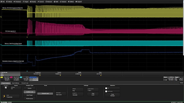
Figure 5: Monitoring the variation of PWM duty cycle during the startup of a power supply. The bottom trace (dark blue) shows the variation in the gate drive duty cycle over the entire startup process. (Image source: DigiKey)
Designers selecting a scope need to be aware that analysis of power converter startup requires an oscilloscope with a long acquisition memory. This example shows a startup acquisition of 10 milliseconds and uses 2.5 megasamples of acquisition memory. The Teledyne LeCroy HDO4000 series scopes can have up to 50 megasamples of acquisition memory. The maximum acquisition time depends on the memory length and the sample period. Acquiring this same data at the minimum required sample rate would provide a 10 second acquisition window for all four channels.
So far we’ve looked at the output side of the power converter. The next two analysis functions look at the primary, or line side of the switched mode converter.
Line power analysis
Line power analysis includes two test functions, power measurements and harmonic analysis. Power measurements determine the line voltage and current. They also measure and display real, apparent, and reactive power. Additionally, the user can choose to calculate and display power factor, phase angle and crest factor. The “Harmonics” test selection measures line harmonics and verifies compliance with international standards like EN 61000-3-2. This compliance test is extremely important to ensure that excessive harmonic power is not injected back into the power mains from the switched-mode device.
Line harmonic analysis is shown in Figure 6. Here, in addition to the line voltage and current in channels C1 and C2 respectively, the first twenty odd harmonics of the 60 Hz line current are displayed in a frequency spectrum display. The blue overlay shows the compliance levels for EN 61000-3-2. The table below the trace display lists each of these harmonics and includes level, frequency, and conformance to the standard.
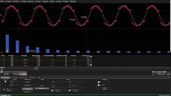
Figure 6: Line harmonic analysis evaluates the harmonic content of the line current using spectrum analysis. Harmonic amplitudes are tested against built-in test masks in conformance with EN 61000-3-2. (Image source: DigiKey)
Having looked at the switching device, control loop, power loss, and input power, the final element of power analysis is overall performance.
Performance analysis
The performance analysis consists of two important tests. The first is device efficiency. This test measures the total input and output power of the switched mode converter under test, and using that information it computes the device efficiency.
The second performance test class is output ripple. This is a really important measurement of power integrity as excessive ripple on the power busses can cause additional jitter in clocks and data signals (Figure 7).
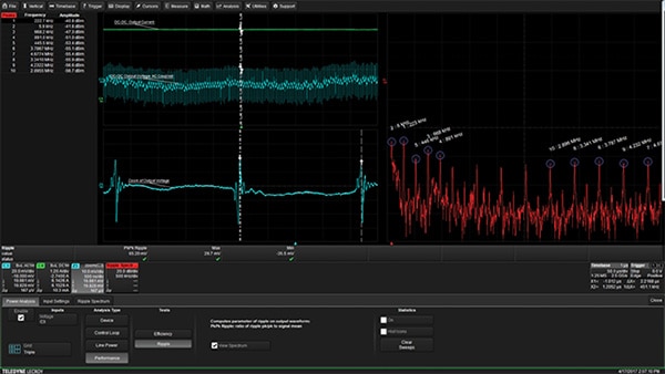
Figure 7: Output ripple is a really important measurement of power integrity. Ripple analysis shows output ripple in both the time and frequency domain. The time view of ripple is shown on the left-hand display traces. The right-hand grid contains the spectrum of the ripple. The table at the extreme left lists the ten highest-frequency components of the ripple. (Image source: DigiKey)
The output current (top left trace) and the AC coupled voltage (left center) are shown in Figure 7. A zoom of the output voltage shows an expanded view of the ripple in the time domain. This ripple is clearly seen to be highly periodic. Cursors measure the basic periodicity as 450 kHz. The ripple parameter lists the peak-to-peak ripple as 65.2 millivolts.
The trace in the right hand grid is the spectrum of the ripple voltage. The table in the upper left corner lists the frequency and amplitude of the ten frequency components with the highest amplitudes. These are also marked on the spectrum display. Knowing the frequency content of the ripple aids the user in determining the possible sources.
Conclusion
Power measurements are getting increasingly complex as applications demand higher efficiency, smaller size and lower cost. As shown, the Teledyne LeCroy HDO4104 with the Power Analyzer software can greatly simplify and shorten test time. Critical measurements of power switching devices, analysis of PWM control loops, and line power efficiency and harmonic testing, are all streamlined with a dedicated user interface and automatic measurements. Also, a wide range of probing solutions with quick and easy setup of voltage and current inputs are available from Teledyne LeCroy.
Using the right equipment and software, power measurements are now as simple as the push of a button.

Disclaimer: The opinions, beliefs, and viewpoints expressed by the various authors and/or forum participants on this website do not necessarily reflect the opinions, beliefs, and viewpoints of DigiKey or official policies of DigiKey.


