Smaller, Higher Performing TVS Diodes Deliver Greater Protection
Contributed By DigiKey's North American Editors
2024-05-22
Electrostatic discharge (ESD) or power surges can damage or fail electronic products during manufacturing or end-use. ESD is estimated to cause anywhere from single digits to a third of all component failures, exacerbated by increased circuit density and higher performance requirements.
Transient voltage events, such as ESD, are hazards that can impact equipment ranging from consumer devices to expensive industrial equipment. The growing reliance on microprocessors that are susceptible to such events and used across a broad spectrum of products, makes it essential to select an appropriate ESD solution to ensure customer satisfaction and commercial success.
When electrons are redistributed on a material surface, they can create a charge imbalance. When the resulting electric field is strong enough, the static charges seek equilibrium and produce an electrostatic discharge. This can be disastrous for microelectronic-based electronics, leading to failure, product delays, revenue loss, and sometimes reputational or brand damage.
Even in a clean IC manufacturing environment, components can be exposed to ESD during processing, assembly, testing, and packaging. The Human Body Model (HBM) is the most widely used testing standard to ensure ICs can withstand the impact of a charged human body—a typical generator of ESD—touching an IC and creating a static charge.
IEC 61000-4-2 is an international ESD testing standard using a human body model at a more substantial system-level hardware benchmark to ensure a device can survive transient events, including lightning protection, when in the hands of real-world end users.
Transient voltage suppression
As integrated circuit geometries continue to shrink, traditional ESD parameters are insufficient to address system-level risks. To protect power and high-speed data circuits, designers must exploit advances in transient voltage suppression (TVS) technology beyond the HBM and on-device ESD protection.
TVS is increasingly essential in protecting against ESD on commonly used data lines for devices with HDMI, Thunderbolt, USB 2, USB 3, USB-C, antennas, and other standard interfaces. Robust protection measures are needed to avoid ESD damage in finished products, ranging from wearables and keyboards to smartphones and IoT cameras.
A TVS diode can be placed on a power or data line to protect against transient events by redirecting surges away from the circuit it safeguards. During a transient event, the voltage on the protected line will quickly rise and can spike to tens of thousands of volts. Under normal operating conditions the TVS diode appears open, but it can arrest a system-level ESD peak in less than a nanosecond, diverting high currents.
Some of the key characteristics in selecting a TVS solution are:
- Capacitance (C) - the inherent ability to store an electrical charge
- Reverse standoff voltage (VRWM)—the maximum voltage that a circuit can operate without activating the TVS diode
- Clamping voltage (VC)—the voltage level at which the TVS begins to divert excess current from the protected circuit (lower than VRWM)
- Reverse breakdown voltage (VBR)—the voltage at which the TVS enters a low impedance mode
- Peak pulse current (IPP)—the maximum current the TVS can handle before becoming damaged
- Peak pulse power (PPP)—the instantaneous power dissipated by the TVS during an event
TVS packaging considerations
The placement of TVS diodes impacts their performance, and close proximity to the ESD entry point provides better protection. Semiconductor packaging also plays a key role in protecting delicate electronics in modern systems against ESD threats.
In selecting TVS diodes for their products, designers should focus on the specific surge protection level desired, the number of lines that need to be protected, and a package size to suit the available board space.
Leaded IC packages are a common option for TVS diodes due to their ease of mounting on printed circuit boards (PCBs), making them cost-effective, and they provide good heat dissipation. Because of their size, however, they can occupy substantial space on the PCB and often have parasitic effects that adversely impact performance.
Fortunately, DFN (Dual Flat No-Lead) packages provide compact dimensions and versatility that may be more suitable for ESD protection. DFN packages do not have extended leads, and their contact points are situated underneath the component rather than along its perimeter, providing space savings compared to leaded surface-mount device (SMD) packaging.
DFN packages provide outstanding heat dissipation by incorporating an exposed thermal pad on the underside that can seamlessly bond with the PCB to function as an integrated heatsink. They also exhibit lower parasitic elements compared to a leaded SMD package, helping to maintain signal integrity in high-speed applications.
DFN packages, though, provide limited visibility of the solder joints on PCBs, which makes it challenging to confirm proper bonding during the post-package assembly process.
Surmounting the DFN challenge
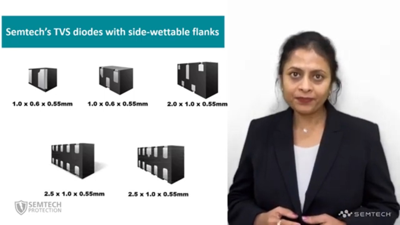
Semtech resolved the DFN challenge with TVS diodes in DFN modules with flip-chip packaging and side-wettable flanks (Figure 1).
 Figure 1: Representative image of Semtech's DFN packaging with side-wettable flanks used for TVS diodes. (Image source: Semtech)
Flip-chip packaging utilizes solder bumps instead of wire bonds to make connections to the substrate. Side-wettable flanks ensure that solder spreads from the bottom of the package, flows up the side of the wall, and forms a visible solder connection.
With this technique, automated visual inspection (AVI) systems can validate proper PCB bonding by visually examining the solder bumps formed between the vertical side of the flank and the solder pad, ensuring reliable connections.
Using side-wettable flanks enhances reliability, improves yield, and provides resistance to vibration and shaking that might otherwise create separation. Tin plating covers the copper terminals, safeguarding the copper from oxidation over time.
Utilizing flip-chip packaging and side-wettable flanks, Semtech introduced a range of single-line TVS diodes packaged in the 0402 size (1.0 mm x 0.6 mm x 0.55 mm) DFN format, tailored for non-automotive industrial applications.
The 0402 DFN TVS components are intended to safeguard against ESD in RF and FM antennas, touchscreen controllers, 12 VDC lines, side-keys and keypads, audio ports, IoT devices, portable instrumentation, general-purpose input-output (GPIO) lines, and industrial equipment.
The Semtech devices provide ESD protection for:
- Thunderbolt 3
- USB 3.0/3.2
- USB Type-C® connectors on high-speed signal lines
- Configuration channel (CC) and sideband use (SBU) lines used for negotiating power, data, and alternate modes connected by USB Type-C cable
- VBus lines
- D+/D- data lines that carry the differential signals for USB and other legacy protocols
Semtech's single-channel, data-line, and VBUS ESD protection solutions with side-wettable flank packaging are available in RClamp and μClamp ESD protection devices. They provide board-level protection with low operating and clamping voltage, fast response time, and no device degradation.
RClamp (RailClamp) products include:
- RCLAMP01811PW.C: Provides designers the flexibility to protect single lines in space-constrained applications such as smartphones, notebooks, and accessories. It can withstand a voltage of ±30 kV (Contact) and ±30 kV (Air) per IEC 61000-4-2, with a low capacitance of 1.2 pF (max). It protects a single line with a working voltage of 1.8 V and a low reverse leakage current of 100 nA (max) at VR = 1.8 V.
- RCLAMP04041PW.C: For protecting single lines in applications where arrays are not practical, such as portable applications with USB 2.0, MIPI/MDDI, MHL, and wearables. With a working voltage of 4.0 V and a low capacitance of 0.65 pF (max), it provides ESD protection for high-speed lines to IEC 61000-4-2 of ±30 kV (Contact & Air) and IEC 61000-4-5 (Lightning) of 20 A (tp = 8/20 µs).
- RCLAMP2261PW.C: A 22 V working voltage, single-line TVS with a surge current of 18 A (tp = 8/20 μs) per IEC 61000-4-5 and a withstand voltage of ±25 kV (Contact) and ±30 kV (Air) per IEC 61000-4-2. Typical applications include USB Type-C, Near-Field Communication (NFC) lines, RF and FM antennas, and IoT Devices.
The ultra-small μClamp (MicroClamp) product line includes:
- UCLAMP5031PW.C: A 5 V working voltage, single-line TVS with withstand voltage of ±30 kV (Contact) and ±30 kV (Air) per IEC 61000-4-2. Designers can utilize it for industrial equipment, portable instrumentation, notebooks, handsets, keypads, and audio ports.
- UCLAMP1291PW.C: A 12 V working voltage, single-line TVS featuring low typical dynamic resistance, low peak ESD clamping voltage, and high ESD withstand voltage of ±30 kV (Contact and Air) per IEC 61000-4-2. Suitable applications include cellular handsets and accessories, notebooks and handhelds, and portable instrumentation.
- UCLAMP2011PW.C: A single-line, 20 V TVS with high lightning surge capability of 3 A (tp=8/20 μs) per IEC 61000-4-5. Typical applications include peripherals, portable devices, and instrumentation.
- UCLAMP2411PW.C: A 24 V, single-line TVS suitable for a broad range of applications including 24 VDC power rails, Chip-on-Glass driver IC data lines, peripherals, and portable devices. It features surge current of 3 A (tp = 8/20 μs) per IEC 61000-4-5.
Conclusion
Increasing circuit density and higher performance for electronic products requires new approaches to protect against electrostatic discharges and other voltage surges. New packaging by Semtech results in smaller transient voltage suppression diodes that provide product designers with greater flexibility, high surge current capability, and low clamping voltages, making them ideal for safeguarding sensitive electronics.
Disclaimer: The opinions, beliefs, and viewpoints expressed by the various authors and/or forum participants on this website do not necessarily reflect the opinions, beliefs, and viewpoints of DigiKey or official policies of DigiKey.