Quickly Create Low-Jitter, High-Frequency Clocks Using a Translation Loop Module
Contributed By DigiKey's North American Editors
2021-08-04
Designers of instrumentation and measurement systems require low-jitter, spurious-free signals in order to provide the signal-to-noise ratios (SNRs) or error vector magnitudes (EVMs) required to meet increasingly demanding customer requirements. At the same time, they are also facing significant pressure to reduce board footprint as well as design cost, and complexity. The latter is critical in to shortening development time to meet narrowing time-to-market windows.
To address the many application challenges, engineers need to transition their instrumentation and measurement clocking solutions from custom-made traditionally discrete designs to more integrated solutions. An important step toward this is to use an integrated translational phase-locked loop (PLL). This allows the frequency up-conversion of a traditional voltage-controlled oscillator (VCO) signal, while substantially maintaining the jitter and phase noise of a fixed external local oscillator (LO).
This article discusses the role of translation loops towards achieving the industry lowest integrated phase noise. By way of example, it introduces the ADF4401A translation loop system-in-package (TL SiP) from Analog Devices and shows how it addresses performance requirements through an output signal with sub-10 femtosecond (fs) rms wideband integrated jitter capability and enhanced isolation to attenuate spurious components, while also meeting designers’ integration, cost, complexity, and time-to-market needs.
Traditional PLL vs. translation loop operations
The primary purpose of a translation loop is to generate an output signal locked to an input reference signal with significantly reduced in-band phase noise compared to traditional PLLs.
A standard PLL consists of a feedback system containing a phase-frequency detector (PFD), charge pump, low-pass filter (LPF), VCO, and a feedback frequency divider N (Figure 1).
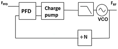 Figure 1: The standard PLL locks to a lower frequency (FPFD) reference and generates an output frequency (FRF). (Image source: Bonnie Baker)
The PFD compares the phase of input reference and the phase of the feedback signal and generates a series of pulses proportional to the phase error between them. The charge pump receives the PFD pulses and converts them into current source or sink pulses that will in turn tune the VCO either up or down in frequency. The LPF removes all the pulses’ high-frequency energy and converts them into a voltage that the VCO can use. The VCO’s output signal is fed back to the PFD block through the N divider to complete the loop.
Figure 1’s frequency transfer function is calculated using Equation 1:
![]() Equation 1
Equation 1
Where FRF is the output frequency
N is the feedback divider ratio (can be integer or fractional)
FPFD is the PFD frequency
Figure 1’s in-band noise floor is calculated using Equation 2:
![]() Equation 2
Equation 2
Where FOMPLL is the PLL’s in-band phase noise floor figure of merit (FOM)
Consider an example with an in-band phase noise floor FOM of -234 decibels per Hertz (dB/Hz); a PFD frequency (FPFD) of 160 megahertz (MHz), and an output frequency (FRF) of 8 gigahertz (GHz).
For this system, Equation 1 is used to calculate the value of N:

Equation 2 is used to calculate the in-band noise floor:

In the calculation above, the N divider strongly contributes to the overall in-band noise floor, with 20 log10 (50), equaling 34 dB. A smaller N value would decrease the in-band noise floor; however, it would also decrease the output frequency. So how do we generate a high output frequency and keep a lower loop gain (N)?
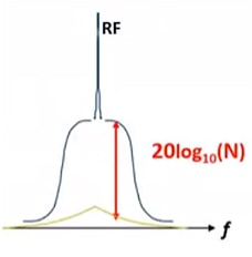 Figure 2: For a standard PLL in this example, the noise from the feedback divider (20 log10(N)) has a 34 dB higher in-band noise compared to the lower yellow plot where N = 1. (Image source: Bonnie Baker)
The solution to this issue is to replace the N-divider with a down-converting mixing stage (Figure 3).
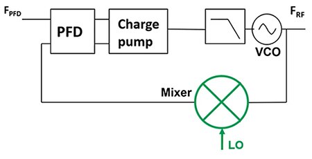 Figure 3: A translation loop uses a mixer to down-convert the VCO frequency to the PFD frequency instead of using a traditional feedback divider. (Image source: Bonnie Baker)
In Figure 3, the mixer replaces the feedback N divider, resulting in a loop gain equal to 1 (N=1). This operation will greatly diminish the contribution of the feedback loop to the in-band noise floor. For the in-band noise calculation, the value of N is now equal to 1. Using Equation 2, the in-band noise floor for the modified system is as follows:

The new in-band noise shows an improvement of 34 dBc/Hz.
In Figure 3, the mixer depends on an extremely low noise LO, called Offset LO. FLO ± FRF must equal FPFD to achieve lock.
With the translation loop architecture, the phase noise of the Offset LO is very important to achieve the best performance at the RF output. For this reason, engineers would typically design an Offset LO based on voltage-controlled surface acoustic wave (SAW), or oscillators (VCSOs), or comb generators, or dielectric resonator oscillators (DROs). NOTE: For support with designing an Offset LO, contact Analog Devices.
Translation loop challenges
Traditionally, the design of a low-noise translation loop involves the implementation of numerous circuit blocks, resulting in a complex design, usually large, and with limited flexibility. In addition, the entire circuit must be validated and characterized for the target operation. For example, one major design concern is LO leakage (LO to RF isolation) to the RF output signal. This is a significant challenge for engineers to address. With traditional designs, engineers usually proceed to multiple design iterations to achieve optimized performance and suitable isolation.
Figure 3 shows how the ADF4401A integrates major circuit blocks to provide a fully characterized solution and eliminates the traditionally difficult areas related to the performance and isolation in translation loop designs. This programmable solution allows engineers to achieve optimized performance on the first effort and reduce time to market.
Evaluating the ADF4401A
The ADF4401A is designed to help engineers reduce the time to market of high-performance instrumentation, using a frequency generation solution with an RF bandwidth of 62.5 MHz to 8 GHz. By using a down-converting mixer, the ADF4401A has very low in-band noise with a wideband jitter of ~9 femtoseconds (fs) integrated from 100 Hz to 100 MHz. The design and layout techniques inside the ADF4401A enable a typical spurious-free dynamic range of 90 dBc. A package size of 18 x 18 x 2.018 millimeters (mm) substantially reduces board space compared to a traditional discrete design.
To evaluate the device’s performance, designers can use the EV-ADF4401ASD2Z evaluation board (Figure 4). The board includes a complete translation loop, including an external PFD (HMC3716), an active filter (LT6200), and a multiplexer (ADG1609).
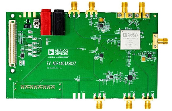 Figure 4: The EV-ADF4401ASD2Z evaluation board for the ADF4401A translation loop module includes an external PFD, a USB interface, and voltage regulators. (Image source: Analog Devices)
The EV-ADF4401ASD2Z includes the ADF4401A TL SiP with integrated VCO, a loop filter (5 MHz), a PFD, a USB interface, and voltage regulators. Additionally, the EV-ADF4401ASD2Z requires the EVAL-SDP-CS1Z (SDP-S) system demonstration platform (SDP) (serial) controller board (Figure 5). The board provides a USB connection from a PC to the EV-ADF4401ASD2Z so it can be programmed. The controller board is not provided in the EV-ADF4401ASD2Z kit.
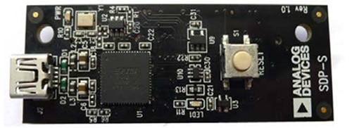 Figure 5: The EVAL-SDP-CS1Z (or SDP-S) controller board is required to provide a USB connection from the EV-ADF4401ASD2Z to a PC for programming. (Image source: Analog Devices)
Figure 6 maps out the physical connections of the EV-ADF4401ASD2Z system. The associated Analysis | Control | Evaluation (ACE) Software controls the TL SiP functions. Power is derived from an externally applied 6-volt power supply.
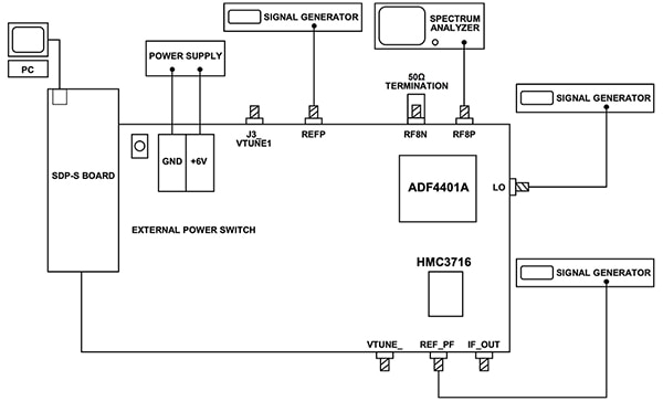 Figure 6: An EV-ADF4401ASD2Z setup diagram shows the equipment and connections required to evaluate the ADF4401A, including the SDP-S control board, PC, power supply, signal generators, and spectrum analyzer. (Image source: Analog Devices)
The suggested equipment to use with this evaluation board includes a Windows PC, a spectrum analyzer or a signal source analyzer, and three signal generators.
The block diagram of the EV-ADF4401ASD2Z shows the ADF4401A module, along with Analog Devices’ HMC3716 PFD, LT6200 op-amp, and the ADG1219 SPDT switch (Figure 7).
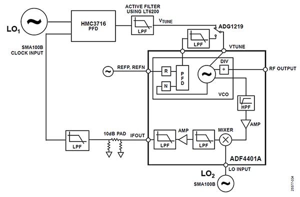 Figure 7: The EV-ADF4401ASD2Z evaluation board block diagram shows the key components supporting the AD4401A translation loop. (Image source: Analog Devices)
It is vital to use a PFD that can operate at high frequencies as this minimizes the need for dividers, which can degrade the in-band noise response. The 1.3 GHz phase comparison frequency capability of Analog Devices’ HMC3716 makes it ideal for use in the IF range of the ADF4401A. The ability of such a circuit to compare both frequency and phase eliminates the need for additional circuitry to steer the frequency to the intended output frequency. The HMC3716 becomes the external PFD to complete the offset loop. The high-frequency operation range and ultra-low phase noise floor of the HMC3716 make it possible to design wide-bandwidth loop filters.
In Figure 7, the LT6200 op-amp with an LPF configuration attenuates high-frequency spurs, while the ADG1219 switch completes the system’s translation loop.
The EV-ADF4401ASD2Z evaluation fixture creates in-band noise plots and jitter measurements as shown in Figure 8.
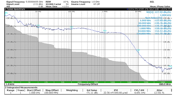 Figure 8: Single sideband phase noise at 5 GHz output, with an external HMC3716 reference of 500 MHz and external LO at 4.5 GHz. (Image source: Analog Devices)
In Figure 8, the LO2 and HMC3716 input is an SMA100B RF and microwave signal generator. The evaluation board’s LO2 in-band noise is approximately -135 dBc/Hz which is apparent at low offsets up to 300 kHz. The LO2, ADF4401A module, HMC3716 PFD, and loop filter contribute to an in-band noise of about -140 dBc/Hz. The internal phase noise appears between 5 MHz and 50 MHz, and the phase noise floor of the fixture is approximately -160 dBc/Hz. These together give an rms jitter of 12.53 fs in total.
Conclusion
High-speed instrumentation systems require extremely low-jitter clocks to ensure that the output data remains uncompromised. The challenge for engineers is to find suitable devices that can build the high-speed gigahertz clock system. The ADF4401A translation loop greatly simplifies device selection to build the clock system, providing a compact module that ensures low jitter at higher frequencies, while also reducing board space, cost, and time to market.

Disclaimer: The opinions, beliefs, and viewpoints expressed by the various authors and/or forum participants on this website do not necessarily reflect the opinions, beliefs, and viewpoints of DigiKey or official policies of DigiKey.


