N+1 Architecture Supports Higher Power Reliability
Contributed By DigiKey's European Editors
2015-08-25
The increased integration made possible by system-on-chip (SoC) devices and high-density field-programmable gate arrays (FPGAs) has made it possible to pack more functionality into industrial systems. However, because these systems now take on roles formerly supported by multiple products, there is an increasing demand for fault tolerance and redundancy not just in the controllers themselves, but also in the power source.
The increased functionality can also lead to high peak current demands. In such cases, the power system designer can use the option of paralleling two or more units. Paralleling not only supports high peak power demands while still offering better overall reliability through less long-term stress; it can support the implementation of ‘n+1’ redundant designs.
The n+1 architecture adds at least one additional power supply to a system that can provide energy if one of the other supplies fails. The n+1 redundancy architecture is particularly cost-effective in larger systems as a way of providing fault tolerance. The probability of more than one power supply failing at once under normal operating conditions is extremely low, so the addition of one additional power supply to an array of two or three running in current-sharing mode does not significantly increase cost.
There are two methods commonly used for n+1 redundancy. One approach is to designate a spare power supply as a cold- or hot-standby. Although cold-standby operation increases the lifetime of the spare power supply, the time it takes to start up after a failure may lead to system failures. Hot standby ensures that the spare is ready to take over in case another power supply in the group fails, but as this supply is operated at extremely low load, and therefore low efficiency, it will suffer greater stress from internal heat generation than a cold-standby unit.
By allowing the spare to take part in current sharing, the stresses on the supplies are balanced across the power-supply subsystem. Traditionally, power supplies have been designed for peak efficiency for high output loads, which means that operating current sharing at less than peak load will increase excess heat generation. However, in recent years, power-supply design has focused on low-load efficiency, making this less of an issue. Supplies that offer a wider high-efficiency range can be used to ensure that the supplies operate in a zone of low heat output during normal operation and move into a higher-load situation after a failure.
Solutions for n+1 redundancy are available at a number of levels, from full-power supplies through to IC-level building blocks. At the level of full-power supplies, the VFK600 series from CUI is designed for parallel operation. When in parallel, the load current can be shared equally between the two modules by connecting their PC pins. The VFK600 can be set up in two different modes to achieve parallel operation, one of them for parallel operation and the other for n+1 redundant operation, suitable for loads when backup power is required.
Providing up to 700 W with an isolated output, the VFK600 is packaged in a rugged metal enclosure with integrated heatsink and is suitable for use with an intermediate DC bus, offering a 2:1 input range from a 18-36 VDC source or 36-77 VDC, converting down to 12 to 48 VDC. The supply offers internal short-circuit protection and remote on/off control.
Although supplies such as the VFK600 contain the necessary componentry to work in n+1 systems, other designs may not, or a custom approach may be required in the power design. As a result, a method is required to safely interconnect multiple power supplies in parallel. One of the commonly used techniques in n+1 designs is to use Schottky ORing diodes to connect redundant power supplies to a common point at the load.
Typically, an ORing device is a diode that is used to protect the system against faults such as short-circuits from the input power source. By allowing current to flow in one direction only, the ORing diode isolates the fault from the redundant bus, allowing the system to keep running using the remaining power supplies.
A diode will effectively disconnect an input power source short circuit instantaneously. However, there are downsides to using a conventional diode. A diode in an ORing application spends most of its operational life in forward-conduction mode, dissipating power and heat due to the diode’s inherent voltage drop, and leading to the need for greater thermal management.
The problem with this higher power dissipation has become more apparent in recent years as power densities have increased and, in applications such as data-center servers, there is a strong drive to reduce the cost of forced air-cooling by as much as possible.
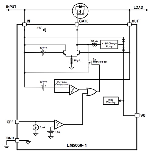
Replacing the ORing diode with an N-channel MOSFET calls for a small increase in the level of complexity, but the greater conductivity of the MOSFET reduces the need for diode heatsinks and similar thermal management techniques in high-power applications at the cost of some additional circuit complexity. An example of a controller designed specifically for this purpose is the Texas Instruments LM5050-1. This is a positive voltage, high-side ORing controller that will drive an external N-channel MOSFET acting as a replacement for an ORing diode.
The voltage across the MOSFET source and drain pins is monitored by the LM5050-1. A ‘gate’ output pin drives the MOSFET to control its operation based on the monitored source-drain voltage. The resulting behavior is that of an ideal rectifier – the source and drain pins of the MOSFET act as the anode and cathode pins of a diode, respectively.

Figure 1: Block diagram of the TI LM5050-1.
The LM5050-1 is designed to regulate the MOSFET gate-to-source voltage if the voltage across the MOSFET source and drain pins falls below approximately 30 mV. As the voltage falls, the gate pin voltage will be decreased until the voltage across the MOSFET is regulated at 22 mV. If the MOSFET current reverses, possibly due to failure of the input supply such that the voltage across the drain and source of the MOSFET is more negative than approximately -30 mV, the LM5050-1 will quickly discharge the MOSFET gate through a strong discharge transistor.
If the input supply fails abruptly, as would occur if the supply would be shorted directly to ground, a reverse current will temporarily flow through the MOSFET until the gate can be fully discharged. This reverse current is sourced from the load capacitance and from the parallel-connected supplies. The LM5050-1 responds to a voltage reversal condition typically within 25 ns. The actual time required to turn off the MOSFET will depend on the charge held by gate capacitance of the MOSFET being used. According to TI, a MOSFET with 47 nF of effective gate capacitance can be turned off in typically 180 ns. This fast turn-off time minimizes voltage disturbances at the output, as well as the current transients from the redundant supplies.
An abrupt zero ohm short circuit across the input supply will cause the highest possible reverse current to flow while the internal LM5050-1 control circuitry discharges the gate of the MOSFET. During this time, the reverse current is limited only by the on-resistance of the MOSFET, together with parasitic wiring resistances and inductances. Worst case instantaneous reverse current would typically be limited to (Vout - Vin)/RDS(on).
When the MOSFET is switched off in such an abrupt fashion, the energy stored in the parasitic wiring inductances will be transferred to the rest of the circuit. As a result, the LM5050-1 will see voltage spikes on the measurement pins. The source-connected pin can be protected by diode clamping the pin to ground in the negative direction; the other pin can be protected with a TVS protection diode, a local bypass capacitor, or both.
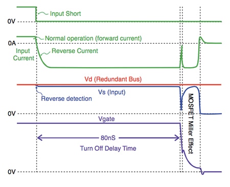
An alternative to discrete active ORing circuitry is to opt for a packaged version, such as the Cool-ORing series of devices from Vicor. These combine a high-speed ORing MOSFET controller and a very low on-state resistance MOSFET in a high-density thermally enhanced 5 x 7 mm land-grid-array (LGA) package. These solutions achieve as low as 1.5 μΩ typical on-state resistance while enabling up to 24 A of continuous load current over a wide range of operating temperature. The design can be used in low-voltage, high-side applications and, by packaging the support circuitry together, can save board space compared with discrete solutions. The components offer responses as fast as 80 nS to fault conditions. A master/slave feature allows the paralleling of devices for high-current active ORing requirements.

Figure 2: Response of the Picor Cool-ORing solution to fault conditions.
By allowing power supplies to be coupled together safely, ORing solutions support the creation of more reliable power systems based on n+1 redundancy at reasonable cost for industrial and similar systems.

Disclaimer: The opinions, beliefs, and viewpoints expressed by the various authors and/or forum participants on this website do not necessarily reflect the opinions, beliefs, and viewpoints of DigiKey or official policies of DigiKey.


