Integrated AFEs, MCUs Simplify Design of Energy-Harvesting Wireless Sensor Nodes
Contributed By Electronic Products
2014-01-29
Energy harvesting has emerged as an effective approach for powering wireless sensor nodes designed to monitor environmental factors. For the sensor subsystems themselves, however, engineers can face significant challenges in building suitable solutions, adding delays to tight project schedules. For many sensor designs, engineers can take advantage of available low-power analog front-ends (AFEs) and specialized MCUs from IC manufacturers including Analog Devices, Cypress Semiconductor, Microchip Technology, and Texas Instruments, among others.
For developing a sensor system, engineers have traditionally relied on building a suitable signal chain by hand, combining op amps, comparators, and related components needed to collect sensor data reliably. Although the concept of acquiring a signal from a sensor seems straightforward, engineers find themselves facing a long list of practical issues such as sensor drive and output requirements, sample rate, signal path calibration, performance, and sensor diagnostics, all within the allotted power budget. Within the signal path itself, challenges associated with component matching, offset trimming, board layout, and nearby noise sources add further complications in building an effective analog signal path.
Signal requirements
Because sensor outputs can be very small signals, sensor signal paths typically require low-noise programmable gain amplifiers (PGAs) with extremely-low offset voltage, as well as low temperature and offset drifts to reduce the chance of introducing errors. In many cases, the common-mode voltage output of the sensor is much larger than the signal of interest, so some designs may require amplifiers with sufficiently high common-mode rejection ratios.
Due to the small sensor signals and overall sensitivity to noise, sensor signal paths also typically include design elements designed to limit the noise floor. These designs typically incorporate filters to limit the signal bandwidth and reduce noise contributions. In addition, chopper-stabilized amplifiers might be used to reduce errors from 1/f noise of the amplifiers. Finally, the use of a ΣΔ ADC with its oversampling conversion method helps reduce noise and associated noise-filtering requirements.
Sensor designs also need to provide a stable excitation voltage or current source with low temperature drift for active sensors such as resistance-temperature detectors (RTDs) and strain gauges. These designs typically provide a ratiometric output where the final output to the MCU is a ratio of the sensor output to the excitation reference voltage, making output effectively immune to variations in the excitation source. Consequently, the excitation reference voltage source does not need to be an expensive high-precision source in most cases.
Integrated AFEs
Traditionally, AFE ICs have combined all the components of the analog signal-conditioning subsystem including op amps, filters, and related circuits in a single package. Today, trends in integration have also placed ADCs on-chip, providing a comprehensive signal chain able to connect a sensor's analog output with an MCU's digital input (Figure 1).

Figure 1: A typical sensor signal chain combines bandwidth-limiting filtering, a low-noise programmable gain amplifier, and an ADC to connect sensors with MCUs (Courtesy of Texas Instruments).
By integrating all the elements of a complete sensor signal path, integrated AFE ICs provide engineers with a near drop-in solution that is already matched, tuned, and qualified to meet performance requirements. In fact, engineers can find integrated AFE ICs designed for specific application segments including communications and medical, among others.
In some cases, AFEs designed for specific segments nevertheless serve more general-purpose sensor applications. Analog Devices notes that their AD73311 AFE for speech and telephony applications is well qualified for general-purpose sensor signal-acquisition designs. The device's 16-bit ADC and low-delay characteristics provide an effective solution for the more general requirements associated with sensor signal acquisition.
Similarly, Analog Device's AD73360 provides a multisensor solution, featuring six 16-bit ADC channels, each providing 77 dB signal-to-noise ratio over a voiceband signal bandwidth. Each channel samples synchronously to reduce delay between the conversions. As a result, even though the AD73360 often finds application in power-metering designs, it is particularly well-suited to multisensor applications requiring synchronized output from diverse sensors.
Microchip Technology's MCP3901 and MCP3911 also serve more general signal-acquisition applications beyond the power-metering designs often targeted with these parts. The MCP3901 dual-channel analog front-end features a high-accuracy 16/24-bit ΣΔ ADC, internal programmable gain amplifiers (PGAs), internal voltage reference, and phase-delay compensation. An MCU can communicate with the MCP3901 through its SPI interface to control the PGAs, resolution, and dithering, as well as to adjust the oversampling ratio for control of the output data rate up to 64 ksamples/s. The MCP3911 AFE provides similar features for 2.7 to 3.6 V applications.
Sensor-specific AFEs
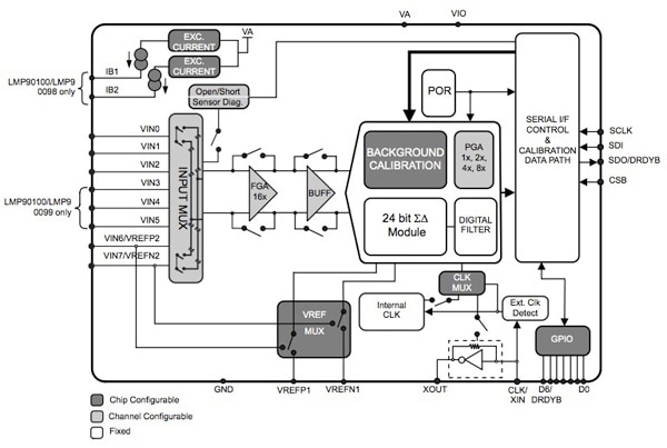
Although many specialized AFEs easily cross over to more general sensor applications, engineers can also find AFEs such as Texas Instruments' LMP AFE series designed specifically for precision sensor signal acquisition. The LMP90100, LMP90099, LMP90098, and LMP90097 are highly-configurable multichannel sensor AFEs providing a complete signal chain built around a 24-bit ΣΔ ADC (Figure 2). While the LMP90100 and LMP90099 offer four differential and seven single-ended inputs, the LMP90098 and LMP90097 offer two differential and four single-ended inputs.

Figure 2: The Texas Instruments LMP90xxx series of integrated AFEs combines a complete sensor signal chain in a configurable architecture designed to adapt easily to specialized requirements (Courtesy of Texas Instruments).
Along with its precision 24-bit ΣΔ ADC, the series includes a low-noise programmable gain amplifier and a fully-differential, high-impedance analog input multiplexer. The devices provide two sets of independent external reference voltage pins for multiple ratiometric measurements. In addition, the LMP90100 and LMP90098 feature two matched programmable current sources from 100 to 1,000 µA to excite external active sensors. Unlike other solutions that typically require periodic recalibration cycles between sample periods, the LMP90xxx series provides a continuous background calibration feature that allows calibration at all gains and output data rates without interrupting the signal path.
ADC alternatives
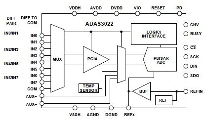
Although the sampling advantages of ΣΔ ADCs are well-suited to many applications that must deal with a noisy sensor environment, the delay and sampling rate limitations inherent in the ΣΔ method may not be effective for other sensor designs. For designs requiring minimal latency in sensor signal conversion, engineers can turn to ICs based on alternative ADC architectures. Analog Devices’ ADAS3022 integrates a 16-bit successive-approximation register (SAR) ADC within a complete signal chain (Figure 3).

Figure 3: The Analog Devices ADAS3022 provides a complete signal-acquisition system based on a successive-approximation register (SAR) ADC, enabling higher-speed signal acquisition than typical ΣΔ ADC-based solutions (Courtesy of Analog Devices).
Microchip offers another integrated AFE providing an alternative to more common ΣΔ ADC-based solutions. Unlike many other AFE architectures, the TC500 offers a precision solution based on a dual-slope ADC. The device contains the integrator, zero-crossing comparator, and processor interface logic, and requires both positive and negative power supplies. The TC500 offers up to 16-bit resolution, 50/60 Hz noise rejection, low-power operation, minimum I/O connections, and low-input bias currents.
MCU-based solutions
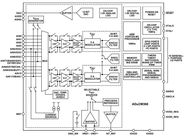
While integrated AFEs provide an MCU-ready output, engineers can also find MCUs designed with a full complement of hardware features needed to build sensor applications. The Analog Devices ADuCM360 is a fully-integrated, 3.9 ksample/s 24-bit data-acquisition system that incorporates dual high-performance, multichannel ΣΔ ADCs, a 32-bit ARM® Cortex™-M3 processor, and Flash/EE memory on a single chip (Figure 4).

Figure 4: Engineers can build sensor subsystems using integrated MCUs such as the Analog Devices ADuCM360, which combines a full analog signal chain on-chip with an ARM Cortex-M3 MCU (Courtesy of Analog Devices).
Designers can interface the ADuCM360 directly with external sensors in both wired and battery-powered applications. Working through an input mux, both ADCs can operate in fully-differential and single-ended modes. The ADuCM360 also integrates dual programmable excitation current sources, diagnostic current sources, and a bias voltage generator to set the common-mode voltage of an input channel.
Alternatively, engineers can build sensor solutions around integrated MCUs such as the CY8C29x66 PSoC series from Cypress Semiconductor. Designers can create user modules that configure the CY8C29x66's on-chip analog resources to implement control amplifiers, trans-impedance amplifiers, ADCs, and other functional blocks required for signal acquisition and conditioning.
Conclusion
Sensor signal-path design can present significant challenges for engineers faced with tight deadlines and stringent performance requirements. In the past, the need to build sensor signal chains "from scratch" using amplifiers, filters, and ADCs has stalled projects as designers struggled to match components, reduce noise, and ensure accurate sensor signal acquisition. Available integrated AFEs and MCUs now provide engineers with a near "drop-in" sensor solution without compromising accuracy for low-power energy-harvesting wireless sensor designs. For more information on the parts mentioned here, use the links provided to access product pages on the DigiKey website.
Disclaimer: The opinions, beliefs, and viewpoints expressed by the various authors and/or forum participants on this website do not necessarily reflect the opinions, beliefs, and viewpoints of DigiKey or official policies of DigiKey.


