How to Use GaN Power Devices for Superior Mid-Range Motor Inverters
Contributed By DigiKey's North American Editors
2024-03-05
The push for more efficient use of energy sources, stricter regulatory mandates, and the technical benefits of cooler operation all support recent initiatives to reduce the amount of power consumed by electric motors. While switching technologies such as silicon MOSFETs are widespread, they often cannot meet the critical inverter applications' more demanding performance and efficiency objectives.
Instead, designers can meet these goals using gallium nitride (GaN), a wide bandgap (WBG) FET device technology that has improved and advanced in terms of cost, performance, reliability, and ease of use. GaN devices are now mainstream and have become the preferred choice for inverters at mid-range power levels.
This article examines how the latest generation GaN-based FETs from Efficient Power Conversion Corporation (EPC) enable high-performance motor inverters. Evaluation boards are presented to help familiarize designers with GaN device characteristics and accelerate designs.
What is an inverter?
An inverter’s role is to create and regulate the voltage waveform that drives a motor, which is often a brushless DC (BLDC) type. It controls motor speed and torque for smooth start and stop, reverse, and acceleration rate, among other requirements. It must also ensure that the desired motor performance is achieved and maintained despite changes in load.
Note that a motor inverter with variable-frequency output should not be confused with an AC-line inverter. The latter takes DC from a source such as a car battery to provide a fixed-frequency 120/240 volt AC waveform, which approximates a sine wave and can be used to power line-operated devices.
Why consider GaN?
GaN devices have attractive attributes relative to silicon, including higher switching speeds, lower drain-source on resistance (RDS(ON)), and better thermal performance. Lower RDS(ON) allows them to be used in smaller and lighter motor drives and reduces power losses, saving energy and cost in applications such as e-bikes and drones. Lower switching losses lead to more efficient motor drives that can extend the range of light electric vehicles (EVs). Faster switching speeds allow for low-latency motor response, essential for applications requiring precise motor control, such as robotics. GaN FETs can also be used to develop more powerful and efficient forklift motor drives. The higher-current handling capabilities of GaN FETs allow them to be used for larger and more powerful motors.
For end applications, the bottom-line benefits are reduced size and weight, higher power density and efficiency, and better thermal performance.
Getting started with GaN
Designing with any power-switching device, especially for mid-range currents and voltages, requires attention to the device’s smallest details and unique characteristics. GaN devices have two internal structure options: depletion mode (d-GaN) and enhancement mode (e-GaN). A d-GaN switch is normally “on” and requires a negative supply; it is more complex to design into circuits. In contrast, e-GaN switches are normally “off” transistors, which results in a simpler circuit architecture.
GaN devices are inherently bidirectional and will start conducting once the reverse voltage across them exceeds the gate threshold voltage. Further, as they are not capable of avalanche mode operation by design, it is critical to have a sufficient voltage rating. A rating of 600 volts is generally adequate at bus voltages up to 480 volts for buck, boost, and bridge DC conversion topologies.
Although GaN switches are simple in their basic on/off power-switching functionality, they are power devices, so designers must give careful consideration to the turn-on and turn-off drive requirements, switching timing, layout, the impact of parasitics, control of current flows, and current-resistance (IR) drops on the circuit board.
For many designers, taking advantage of evaluation kits is the most effective way to understand what GaN devices can do and how to use them. These kits use individual and multiple GaN devices in different configurations and power levels. They also include the associated passive components, including capacitors, inductors, resistors, diodes, temperature sensors, protection devices, and connectors.
Start with lower-power devices
An excellent example of a lower-power GaN FET is the EPC2065. It has a drain-source voltage (VDS) of 80 volts, a drain current (ID) of 60 amperes (A), and an RDS(ON) maximum of 3.6 milliohms (mΩ). It is supplied only in passivated die form with solder bars and measures 3.5 × 1.95 millimeters (mm) (Figure 1).
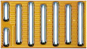 Figure 1: The 80 volt, 60 A EPC2065 GaN FET is a passivated die device with integral solder bars. (Image source: EPC)
As with other GaN devices, the EPC2065’s lateral device structure and majority carrier diode provide exceptionally low total gate charge (QG) and zero reverse recovery charge (QRR). These attributes make it a good fit for situations where very high switching frequencies (up to several hundred kilohertz) and low on-time are beneficial, as well as those situations where on-state losses dominate.
This device is supported by two similar evaluation kits: the EPC9167KIT for 20 A/500 watt operation, and the higher-power EPC9167HCKIT for 20 A/1 kilowatt (kW) operation (Figure 2). Both are three-phase BLDC motor-drive inverter boards.
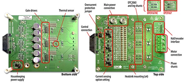 Figure 2: Shown are the bottom (left) and top (right) of the EPC9167 board. (Image source: EPC)
The basic EPC9167KIT configuration uses a single FET for each switch position and can deliver up to 15 ARMS (nominal value) and 20 ARMS (peak value) of current per phase. In contrast, the higher-current EPC9167HC configuration uses two parallel FETs per switch position and can deliver maximum currents up to 20 ARMS/30 ARMS (nominal/peak) output current, demonstrating the relative ease with which GaN FETs can be configured in parallel for higher output current. A block diagram of the base EPC9167 board is shown in Figure 3.
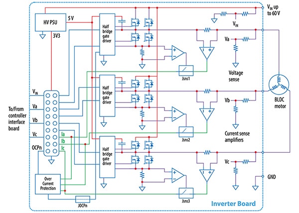 Figure 3: Shown is a block diagram of the base EPC9167 board in a BLDC drive application; the higher-power EPC9167HC has two EPC2065 devices in parallel for each switch, while the lower-power EPC9167 has only one FET per switch. (Image source: EPC)
The EPC9167KIT contains all the critical circuits to support a complete motor-drive inverter, including gate drivers, regulated auxiliary power rails for housekeeping supplies, voltage sense, temperature sense, current sense, and protection functions.
The EPC9167 mates with assorted compatible controllers and is supported by various manufacturers. It can be swiftly configured as a motor-drive inverter by leveraging existing resources for quick development.
Going to higher power
At the other end of the power-handling range is the EPC2302, a GaN FET featuring a 100 volt/101 A rating and just 1.8 mΩ RDS(ON) maximum. It is well-suited to high-frequency DC-DC applications from 40 to 60 volts and 48 volt BLDC motor drives. In contrast to the passivated die packaging with solder bars used for the EPC2065, this GaN FET is housed in a low-inductance QFN package measuring 3 × 5 mm with an exposed top for superior thermal management.
The thermal resistance to the case top is low, at just 0.2°C per watt, resulting in excellent thermal behavior and eases cooling challenges. Its exposed top enhances top-side thermal management, while the side-wettable flanks guarantee that the complete side-pad surface is wetted with solder during the reflow soldering process. This protects the copper and allows soldering on this external flank area for easy optical inspection.
The footprint of the EPC2302 is less than half the size of the best-in-class silicon MOSFET with similar RDS(on) and voltage ratings, while its QG and QGD are significantly smaller, and its QRR is zero. This results in lower switching losses and lower gate driver losses. The EPC2302 operates with a short deadtime of in the tens of nanoseconds (ns) for higher efficiency, while its zero-value QRR enhances reliability and minimizes electromagnetic interference (EMI).
To exercise the EPC2302, the EPC9186KIT Motor Controller/Driver Power Management Evaluation Board supports motors up to 5 kW and can deliver up to 150 ARMS and 212 APEAK maximum output current (Figure 4).
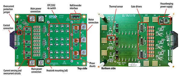 Figure 4: Shown are the top (left) and bottom (right) of the EPC9186KIT 5 kW evaluation board for the EPC2302. (Image source: EPC)
To achieve this higher current rating, the EPC9186KIT uses four parallel GaN FETs per switch position, demonstrating the ease of using this approach to reach higher current levels. The board supports PWM switching frequencies up to 100 kHz in motor-drive applications, and contains all the critical functions to support a complete motor-drive inverter, including gate drivers, regulated auxiliary housekeeping power supplies, voltage and temperature sensing, accurate current sense, and protection functions.
Conclusion
Motor inverters are the critical link between a basic power source and a motor. Designing smaller, higher-efficiency and higher-performance inverters is an increasingly important objective. While designers have choices in process technology for the critical power-switching devices mid-range inverters use, GaN devices, such as those from EPC, are the preferred option.

Disclaimer: The opinions, beliefs, and viewpoints expressed by the various authors and/or forum participants on this website do not necessarily reflect the opinions, beliefs, and viewpoints of DigiKey or official policies of DigiKey.


