How to use FPGA SoCs for Secure and Connected Hard Real-Time Systems
Contributed By DigiKey's North American Editors
2023-02-16
Field programmable gate arrays (FPGAs), Linux-capable RISC-V microcontroller unit (MCU) subsystems, advanced memory architectures, and high-performance communications interfaces are important tools for designers. This is particularly true for designers of secure connected systems, safety-critical systems, and a wide range of hard real-time deterministic systems like artificial intelligence (AI) and machine learning (ML).
However, the integration of those diverse elements into a secure, connected, and deterministic system can be a challenging and time-consuming activity, as is laying out the high-speed interconnects for the various system elements. Designers need to include a memory management unit, memory protection unit, secure boot capability, and gigabit-class transceivers for high-speed connectivity. The design will need active and static power management and control of inrush currents. Some designs will require operation over the extended commercial temperature range of 0°C to +100°C junction temperature (TJ), while systems in industrial environments will need to operate with TJ from -40°C to +100°C.
To address these and other challenges, designers can turn to FPGA system-on-chip (SoC) devices that combine low power consumption, thermal efficiency, and defense-grade security for smart, connected, and deterministic systems.
This article reviews the architecture of such an FPGA SoC and how it supports the efficient design of connected and deterministic systems. It then briefly presents the EEMBC CoreMark-Pro processing power versus power consumption benchmark, along with a view of the benchmark performance of a representative FPGA SoC. It looks at how security is baked into these FPGA SoCs and details exemplary FPGA SoCs from Microchip Technology, along with a development platform to accelerate the design process. It closes with a brief listing of expansion boards from MikroElektronika that can be used to implement a range of communications interfaces, as well as global navigation satellite system (GNSS) location capability.
SoCs built with an FPGA fabric
The ‘chip’ for this SoC is an FPGA fabric that contains the system elements, from the FPGA to the RISC-V MCU subsystem that’s built with hardened FPGA logic. The MCU subsystem includes a quad-core RISC-V MCU cluster, a RISC-V monitor core, a system controller, and a deterministic Level 2 (L2) memory subsystem. The FPGA in these SoCs includes up to 460 K logic elements, up to 12.7 gigabit per second (Gbps) transceivers, and other input/output (I/O) blocks, including general purpose I/O (GPIO) and Peripheral Component Interconnect Express (PCIe) 2. The overall architecture is designed for reliability. It includes single-error correction and double-error detection (SECDED) on all memories, differential power analysis (DPA), physical memory protection, and 128 kilobits (Kbits) of flash boot memory (Figure 1).
") Figure 1: All the elements in this FPGA SoC, including the RISC-V subsystems, are implemented on the FPGA fabric. (Image source: Microchip Technology)
Figure 1: All the elements in this FPGA SoC, including the RISC-V subsystems, are implemented on the FPGA fabric. (Image source: Microchip Technology)
Microchip offers its Mi-V (pronounced “my five”) ecosystem of third-party tools and design resources to support the implementation of RISC-V systems. It’s built to speed the adoption of the RISC-V instruction set architecture (ISA) for hardened RISC-V cores and for RISC-V soft cores. Elements of the Mi-V ecosystem include access to:
- Intellectual property (IP) licenses
- Hardware
- Operating systems and middleware
- Debuggers, compilers, and design services
The hardened RISC-V MCUs in the FPGA SoC include several debugging capabilities like passive run-time configurable advanced extensible interface (AXI) and instruction trace. AXI enables designers to monitor data that’s being written to or read from various memories and to know when it’s being written or read.
The RISC-V MCU subsystem uses a five-stage single-issue, in-order pipeline. It’s not vulnerable to Spectre or Meltdown exploits that can afflict out-of-order architectures. All five MCUs are coherent with the memory subsystem, supporting a mix of deterministic asymmetric multi-processing (AMP) mode real-time systems and Linux. Capabilities of the RISC-V subsystem include (Figure 2):
- Run Linux and hard real-time operations
- Configure L1 and L2 as deterministic memory
- DDR4 memory subsystem
- Disable/enable branch predictors
- In-order pipeline operation
 Figure 2: The RISC-V subsystem includes several processor and memory elements. (Image source: Microchip Technology)
More processing with less energy
In addition to their system operation benefits, including support for hard, real-time processing, these FPGA SoCs are highly energy efficient. The EEMBC CoreMark-PRO benchmark is an industry standard for comparing the efficiency and performance of MCUs in embedded systems. It was designed specifically to benchmark hardware performance and to replace the Dhrystone benchmark.
The CoreMark-PRO workloads include a diversity of performance characteristics, instruction-level parallelism, and memory utilization based on four floating-point workloads and five common integer workloads. The floating-point workloads include a linear algebra routine derived from LINPACK, a fast Fourier transform, a neural net algorithm for pattern evaluation, and an improved version of the Livermore loops benchmark. JPEG compression, an XML parser, ZIP compression, and a 256-bit secure hash algorithm (SHA-256) form the basis of the integer workloads.
The MPFSO95T models of these SoC FPGAs, like the MPFS095TL-FCSG536E, can deliver up to 6,500 Coremarks at 1.3 watts (Figure 3).
 Figure 3: The MPFS095T FPGA SoC (orange line) delivers 6500 Coremarks at 1.3 watts. (Image source: Microchip Technology)
Security considerations
The safety-critical and hard real-time applications for these FPGA SoCs require strong security in addition to high energy efficiency and powerful processing capabilities. The basic security functions of these FPGA SoCs include differential power analysis (DPA) resistant bitstream programming, a true random number generator (TRNG), and a physically unclonable function (PUF). They also include standard and user-defined secure boot, physical memory protection that provides memory access restrictions related to the machine’s privilege state, including machine, supervisor, or user modes, and immunity from Meltdown and Spectre attacks.
Security begins with secure supply chain management, including the use of hardware security modules (HSMs) during wafer testing and packaging. The use of a 768-byte digitally signed x.509 FPGA certificate embedded in every FPGA SoC adds to supply chain assurance.
Numerous on-chip tamper detectors are included in these FPGA SoCs to ensure secure and reliable operation. If tampering is detected, a tamper flag is issued that enables the system to respond as needed. Some of the available tamper detectors include:
- Voltage monitors
- Temperature sensors
- Clock glitch and clock frequency detectors
- JTAG active detector
- Mesh active detector
Security is further ensured with 256-bit advanced encryption standard (AES-256) symmetric block cipher correlation power attack (CPA) countermeasures, integrated cryptographic digest capabilities to ensure data integrity, integrated PUF for key storage, and zeroization capabilities for the FPGA fabric and all on-chip memories.
FPGA SoC examples
Microchip Technology combines these capabilities and technologies into its PolarFire FPGA SoCs with multiple speed grades, temperature ratings, and various package sizes to support designers’ needs for a wide range of solutions with between 25 K and 460 K logic elements. Four temperature grades are available (all rated for TJ), 0°C to +100°C extended commercial range, -40°C to +100°C industrial range, -40°C to +125°C automotive range, and -55°C to +125°C military range.
Designers can choose from standard speed grade devices, or -1 speed grade devices that are 15% faster. These FPGA SoCs can be operated at 1.0 volt for lowest power operation, or at 1.05 volts for higher performance. They are available in a range of package sizes, including 11 x 11 millimeters (mm), 16 x 16 mm, and 19 x 19 mm.
For applications that need extended commercial temperature operation, standard speed operation, and 254 K logic elements in a 19 x 19 mm package, designers can use the MPFS250T-FCVG484EES. For simpler solutions that need 23 K logic elements, designers can turn to the MPFS025T-FCVG484E, also with extended commercial temperature operation and standard speed grade in a 19 x 19 mm package. The MPFS250T-1FCSG536T2 with 254 K logic elements is designed for high-performance automotive systems and has an operating temperature range of -40 to 125°C and a -1 speed grade for a 15% faster clock, in a compact 16 x 16 mm package with 536 balls on a 0.5 mm pitch (Figure 4).
 Figure 4: The automotive temperature MPFS250T-1FCSG536T2 comes in a 16 x 16 mm package with a ball count of 536 and a 0.5 mm pitch. (Image source: Microchip Technology)
FPGA SoC dev platform
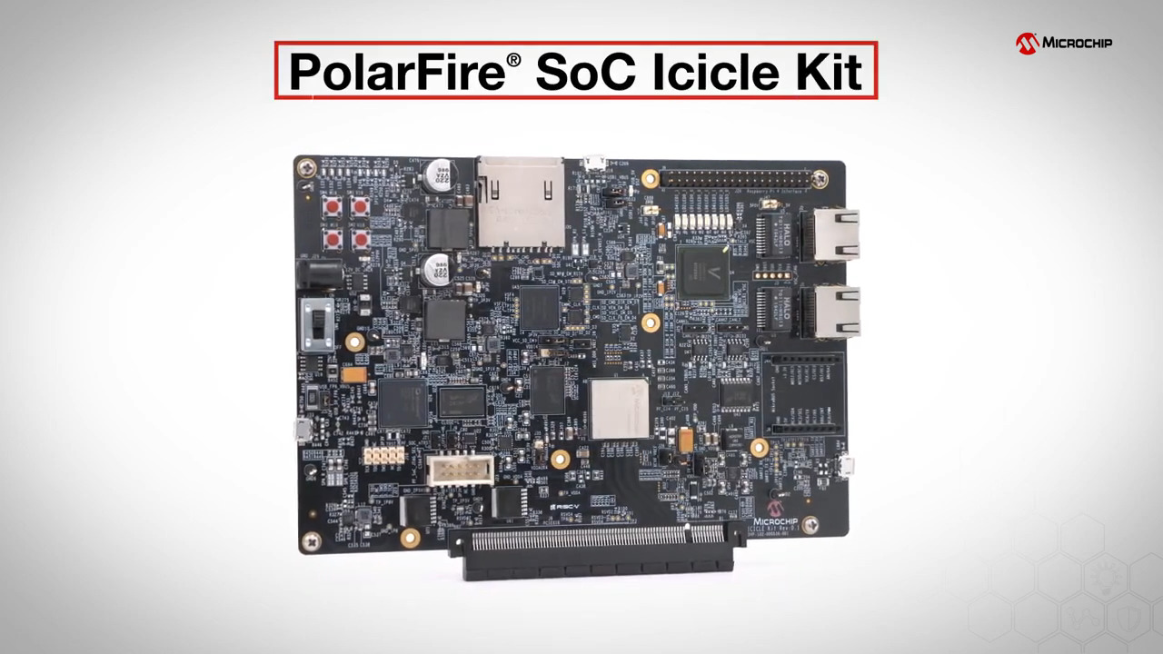
To speed the design of systems with the PolarFire FPGA SoC, Microchip offers the MPFS-ICICLE-KIT-ES PolarFire SoC Icicle kit that enables exploration of the five-core Linux-capable RISC-V microprocessor subsystem with low-power, real-time execution. The kit includes a free Libero Silver license that’s needed to evaluate designs. It supports programming and debugging features in a single language.
These FPGA SoCs are supported with the VectorBlox accelerator software development kit (SDK) that enables low-power, small-form-factor AI/ML applications. The emphasis is on simplifying the design process to the point that designers don’t need to have prior FPGA design experience. The VectorBlox accelerator SDK enables developers to program power-efficient neural networks using C/C++. The Icicle kit has numerous features to provide a comprehensive development environment, including a multi-rail power sensor system to monitor the various power domains, PCIe root port, and on-board memories—including LPDDR4, QSPI, and eMMC Flash—to run Linux and Raspberry Pi, and mikroBUS expansion ports for a host of wired and wireless connectivity options, plus functional extensions like GNSS location capability (Figure 5).
") Figure 5: This comprehensive FPGA SoC development environment includes connectors for Raspberry Pi (top right) and mikroBUS (lower right side) expansion boards. (Image source: Microchip Technology)
Figure 5: This comprehensive FPGA SoC development environment includes connectors for Raspberry Pi (top right) and mikroBUS (lower right side) expansion boards. (Image source: Microchip Technology)
Expansion boards
A few examples of mikroBUS expansion boards include:
MIKROE-986, for adding CAN bus connectivity using a serial peripheral interface (SPI).
MIKROE-1582, for interfacing between the MCU and an RS-232 bus.
MIKROE-989, for connecting with an RS422/485 communication bus.
MIKROE-3144, supports the LTE Cat M1 and NB1 technologies enabling reliable and simple connectivity with 3GPP IoT devices.
MIKROE-2670, enables GNSS functionality with concurrent reception of GPS and Galileo constellations plus either BeiDou or GLONASS, resulting in high position accuracy in situations with weak signals or interference in urban canyons.
Conclusion
Designers can turn to FPGA SoCs when developing connected, safety-critical and hard real-time deterministic systems. FPGA SoCs provide a wide range of system elements, including an FPGA fabric, RISC-V MCU subsystem with high-performance memories, high-speed communications interfaces, and numerous security functions. To help designers get started, development boards and environments are available that include all the necessary elements, including expansion boards that can be used to implement a wide range of communications and location functions.
Recommended reading
Disclaimer: The opinions, beliefs, and viewpoints expressed by the various authors and/or forum participants on this website do not necessarily reflect the opinions, beliefs, and viewpoints of DigiKey or official policies of DigiKey.