How to Reduce Losses, Improve Efficiency, and Extend Temperature Range in High-Power Applications
Contributed By DigiKey's North American Editors
2023-09-08
Designers of power-intensive applications require smaller, lighter, and more efficient power converters, able to operate at higher voltages and temperatures. This is particularly true in applications like electric vehicles (EVs) where such improvements translate to faster charging and greater range. To achieve these improvements, designers are using power converters based on wide bandgap (WBG) technologies such as silicon carbide (SiC).
Compared to silicon (Si), these devices operate at higher voltages and weigh less, yet have similar power-handling capabilities. They also operate at higher temperatures, reducing cooling system needs. SiC devices can operate at a higher switching frequency, allowing the use of smaller passive components that reduce converter size and weight. Still, SiC is under constant development, with more recent efforts resulting in lower “on” resistance, further reducing power losses.
This article briefly discusses the advantages of SiC over Si, using EVs for context. It then discusses SiC developments before introducing ROHM Semiconductor’s 4th generation SiC MOSFETs, and illustrating how they help designers reduce power losses, cost, and footprint
Why use SiC?
EVs need increased battery capacity for greater range. In conjunction with this trend, battery voltages are being increased to 800 volts in order to reduce charging time. As a result, designers of EVs need devices that can withstand these higher voltages and, at the same time, reduce electrical losses and weight. ROHM Semiconductor’s 4th generation SiC MOSFETs deliver lower losses through higher voltage tolerance, lower conduction and switching losses, and smaller sizes.
SiC, a WBG semiconductor, offers exceptional efficiency in high-voltage power switching applications relative to Si MOSFET technology. A comparison of the physical properties of SiC and Si shows the source of this improvement based on five physical properties: breakdown electric field, bandgap, thermal conductivity, and melting point (Figure 1).
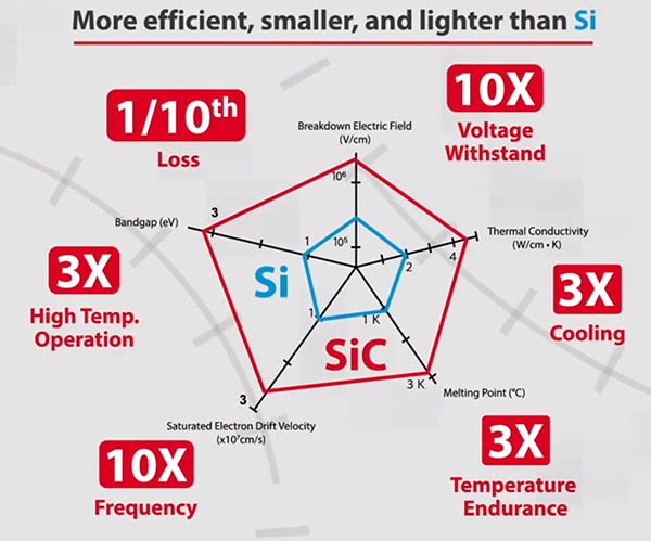 Figure 1: Shown are the advantages of SiC over Si MOSFETs based on five physical properties. (Image source: ROHM Semiconductors)
The breakdown electric field strength of SiC is ten times greater than that of Si, making it possible to design devices with higher breakdown voltages while reducing the device thickness. The wider bandgap of SiC permits the device to operate at much higher temperatures. Higher thermal conductivity reduces the effort needed to cool the device, while the higher melting point increases the operating temperature range. Finally, the higher saturated electron drift velocity of SiC results in higher possible switching frequencies and lower switching losses. These higher switching frequencies require smaller filters and other passive components, further reducing size and weight.
MOSFET development
The original SiC MOSFETs used a planar structure where the device gate and channel are on the surface of the semiconductor. Planar devices are limited in their component density as there is a limit to how much designs can be reduced in size in an attempt to improve device yield. The use of single and double-trench MOSFETs offers the ability to achieve higher device densities (Figure 2).
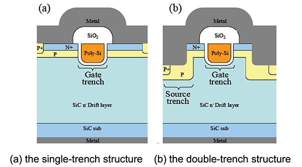 Figure 2: Trench MOSFETs achieve higher device densities by arranging the device elements vertically. (Image source: ROHM Semiconductor)
Like other MOSFETs, a trench MOSFET cell contains the drain, gate, and source, but is arranged vertically. The channel forms vertically, parallel to the gate trench, by means of the field effect. The direction of current flow is vertical from source to drain. Compared to a planar device, which is spread horizontally and takes a good deal of surface area, this structure is very compact.
The single-trench structure uses a single-gate trench. The double-trench device has both a gate and a source trench. ROHM Semiconductor switched to the double-trench structure for its 3rd generation SiC MOSFETs. The 4th generation design advanced the double-trench design by decreasing the cell size, further reducing the on-state resistance and parasitic capacitance, leading to much lower power losses and providing the option to use smaller SiC devices for more cost-effective system designs.
Lowering the on-state resistance of a MOSFET may compromise its ability to handle short circuits. However, the 4th generation SiC MOSFET achieves lower on resistance without sacrificing the short-circuit withstand time, giving these devices a significant advantage when it comes to achieving both high efficiency and robust short-circuit ruggedness.
Understanding losses
Losses in a switched-mode converter come from several sources; those associated with the active devices include conduction, switching, and body diode losses (Figure 3).
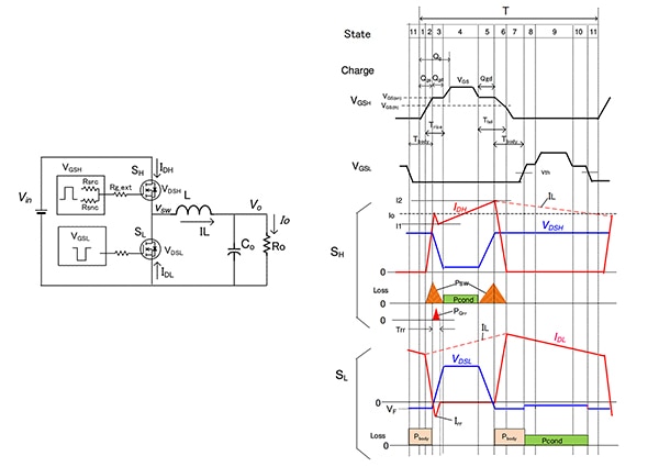 Figure 3: Shown is a schematic of a buck DC/DC converter labeled to show the switching waveforms and the associated loss waveforms. (Image source: ROHM Semiconductor)
The buck converter uses a totem pole design with a high-side (SH) and a low-side (SL) MOSFET switch. The switches are driven out of phase so that only one conducts at a time. The gate drive waveforms (VGSH and VGSL) show the amplitude steps due to the associated charging intervals for the device’s parasitic capacitances. The drain-to-source voltage (VDSH, VDSL) and drain current (IDH, IDL) waveforms for both devices are shown. When the device is on, the VDS is low. When the device is off, the VDS is high. During the time when the SH is on, the drain current increases linearly while it charges the magnetic field of the inductor. During this time, the current through the channel resistance develops a voltage across the channel, resulting in conduction losses (PCOND) that are proportional to the square of the current and the channel on resistance. During the intervals in which the device changes state, the voltage and current are both non-zero, and power is dissipated in the device proportional to the voltage, current, switching transition time, and switching frequency. These are the switching losses.
A similar situation occurs when SL is on. Here, the current decreases linearly as the energy stored in the inductor provides the drain current in the lower device. Again, the channel resistance dissipates power as a conduction loss. Note that the VDSL in the lower device is near zero before the current becomes non-zero, so there are no switching losses associated with this part of the cycle.
The recovery loss (PQrr) is caused by the recovery of the body diode of the devices; for simplicity, it is shown only for the high side.
Pbody is the body diode conduction of the devices. This loss is generated by the current conducted through the body diode of the low-side device.
The total power loss is the sum of all these components for both transistors.
Improved performance of 4th generation SiC MOSFETs
A comparison of the performance of Si IGBT as well as 3rd and 4th generation SiC MOSFETs, was conducted using a 5 kilowatt (kW) full-bridge inverter (Figure 4). In this full-bridge circuit, the switching devices are connected in parallel for higher current capability. The full bridge uses a total of eight devices. The eight devices are shown mounted on the heatsink of the left image. The efficiency of the circuit was evaluated using the original IGBT and the 3rd and 4th generation MOSFETs. The inverter operates at a 40 kilohertz (kHz) switching frequency with the SiC MOSFETs and at 20 kHz with the IGBT.
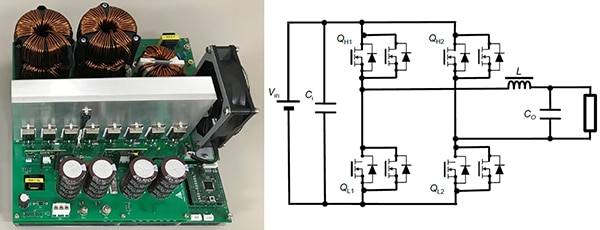 Figure 4: Shown are a 5 kW fanless inverter and its schematic. Originally designed with silicon IGBTs running at 20 kHz, this circuit was run with both 3rd and 4th generation SiC MOSFETs at 40 kHz. The performance of all three semiconductor types was compared. (Image source: ROHM Semiconductor)
The 3rd generation device was a ROHM Semiconductor SCT3030AL device rated at 650 volts with a channel resistance (RDS(ON)) of 30 milliohms (mΩ). The 4th generation MOSFET was a ROHM Semiconductor SCT4026DEC11. The voltage rating on the 4th generation device was increased to 750 volts. Its RDS(ON) is 26 mΩ, a 13% reduction that slightly reduced conduction losses.
A comparison of both SiC MOSFETs losses with those of the original IGBT shows the improvement in efficiency (Figure 5).
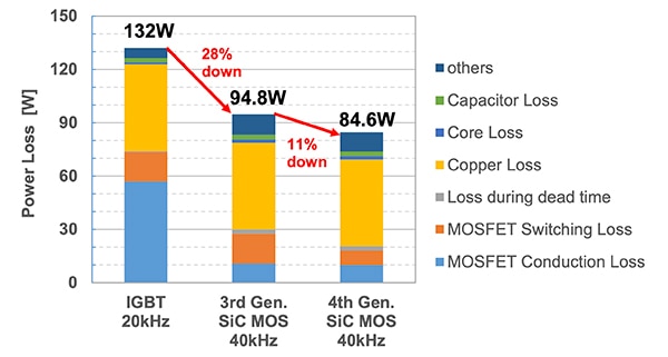 Figure 5: The 4th generation SiC MOSFETs significantly reduced losses compared to the original Si IGBT and the 3rd generation device. (Image source: ROHM Semiconductor)
The 4th generation device reduced conduction losses (blue) from 10.7 to 9.82 watts compared with the 3rd generation device. A more significant reduction was achieved with switching losses (orange), a decrease from 16.6 to 8.22 watts.
Additional improvements in the 4th generation devices include improved gate drive capabilities. The 4th generation SiC MOSFETs support driving with 15 volts; 3rd generation devices require 18 volts. This means that circuits designed with Si devices can use 4th generation MOSFETs as drop-in replacements. In addition, the recommended drive voltage during turn-off is 0 volts for the 4th generation SiC MOSFETs. Prior to the 4th generation products, the gate-to-source voltage needed a negative bias during turn-off to prevent self-turn-on. However, in the 4th generation devices, the threshold voltage (Vth) is designed to be high in order to suppress the self-turn-on, eliminating the need for the application of negative bias.
4th generation solutions
ROHM Semiconductor’s 4th generation SiC MOSFET solutions break down into two groups based on the device package. The SCT4026DEC11, which was discussed, is a 750-volt, 56 ampere (A) (+25°C)/29 A (+100°C), 26 mΩ SiC MOSFET in a three-lead TO-247N package. An example of the alternative four-lead package is the SCT4013DRC15, a 750 volt, 105 A (+25°C)/74 A (+100°C), 13 mΩ device in a four-lead TO-247-4L package.
The four-lead package adds an extra lead that improves the switching speed of the MOSFET. The conventional TO-247N three-pin package does not isolate the gate drive from the parasitic source-lead inductance due to high drain current. The gate voltage is applied between the gate and source pins. The effective gate voltage at the chip is reduced due to the voltage drop across the parasitic inductance (VL) of the source terminal, causing the switching speed to be reduced (Figure 6).
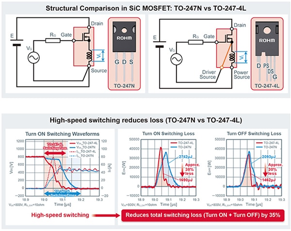 Figure 6: The fourth pin on the TO-247-4L isolates the gate drive from the power source pins using an additional connecting pin in a Kelvin connection. (Image source: ROHM Semiconductor)
The four-pin TO-247-4L package splits the gate drive and power source pins connecting the gate drive directly to the source internally. This minimizes the effects of the parasitic inductance of the source pin. The direct connection of the gate drive to the internal source connection makes it possible to maximize the switching speed of SiC MOSFETs, reducing total switching loss (turn ON and turn OFF) by up to 35% compared to the conventional three-pin TO-247N packages.
The second differentiating specification for the 4th generation SiC MOSFETs is the voltage rating. Devices are available with voltage ratings of 750 volts or 1200 volts. The two devices discussed so far have voltage ratings of 750 volts. For higher voltage applications, the SCT4062KEC11 is a 1200 volt, 62 mΩ, 26 A (+25°C)/18 A (+100°C) SiC N-channel MOSFET in a three-lead TO-247N package, while the SCT4036KRC15 is a 1200 volt, 36 mΩ, 43 A (+25°C)/30 A (+100°C) N-channel MOSFET in a four-lead TO-247-4L package. In total, there are currently ten 4th generation SiC MOSFETs available, with current ratings of from 26 A to 105 A at +25°C. They have RDS(ON) values ranging from 13 to 62 mΩ.
EV applications
4th generation SiC MOSFET specifications are well matched to EV applications. Battery EVs (BEVs) with voltages of 400 or 800 volts provide an example (Figure 7).
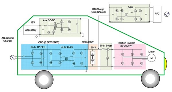 Figure 7: Typical 4th generation SiC MOSFET applications within a BEV and associated external accessories. (Image source: ROHM Semiconductor)
Figure 7 shows a block diagram of a BEV with a 400- or 800-volt battery voltage, supporting both bi-directional and fast charging. The onboard charger (OBC) includes totem-pole power factor correction circuits (PFCs) and a bidirectional, full-bridge CLLC (capacitor, inductor, inductor, capacitor) resonant converter. The external ‘Quiq’ charge DC charger provides direct charging to the battery. The battery drives the traction inverter, which converts DC into three-phase AC to drive the motor. All these circuits employ MOSFETs in various circuit configurations to handle the power levels required. 4th generation SiC MOSFETs are important because they reduce circuit physical size and increase voltage rating while reducing losses and costs.
Conclusion
For designers of high-voltage, high-power applications, including EVs, data centers, and base stations, 4th generation SiC MOSFETs are key power-switching devices. As shown, they use a unique structure to greatly improve power conversion efficiency by reducing losses, while also reducing footprint and cost.
Recommended Reading:

Disclaimer: The opinions, beliefs, and viewpoints expressed by the various authors and/or forum participants on this website do not necessarily reflect the opinions, beliefs, and viewpoints of DigiKey or official policies of DigiKey.


