How to Optimize SWaP in High-Performance RF Signal Chains
Contributed By DigiKey's North American Editors
2022-10-20
The demand for high-performance wireless connectivity continues to increase across a widening array of applications, from smartphones to laptops, tablets, wearables, drones, access points, and smart home and Internet of Things (IoT) enabled appliances. For designers of these devices, a critical differentiator is the end-user experience, which in large part is determined by the quality, throughput, and reliability of the wireless signal, as well as the battery life. Device size and weight are also important differentiators, particularly in wearables. For designers, optimizing for these parameters requires a close look at all aspects of the radio frequency (RF) signal chain, which can be a daunting challenge for both experts and RF novices alike.
This article reviews various parts of the RF signal chain and describes how antenna tuners, RF cross switches, antenna diversity switches, low-noise amplifiers (LNAs), and low-noise RF transistors contribute to high-performance solutions, as well as looking at control interface options. It then presents exemplary components from Infineon and shows how they support high-performance RF designs while meeting increasingly demanding size, weight, and power (SWaP) requirements. It closes by comparing two small, non-leaded package (TSNP) options for compact RF solutions.
Antenna essentials
Antenna performance is critical in today’s connected devices. Tuning can enable a single antenna to provide good performance in several frequency bands and contribute to a more compact and efficient solution. Designers can use switches in the antenna tuner section of the RF signal chain to maximize power transfer to the antenna and optimize performance as demanded by the specific application requirements (Figure 1).
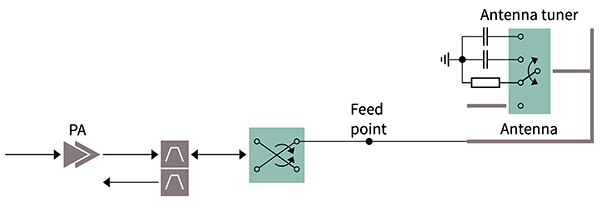 Figure 1: Antenna tuning switches are used in the tuner section to optimize antenna performance. (Image source: Infineon)
RF cross switches
In many applications, antenna tuning is a necessary but not sufficient condition to ensure optimal performance. In those cases, more than one antenna may be needed. An RF cross switch can be added to the signal chain to enable the selection of the antenna that provides the best performance in a given situation by increasing transmit power or receiver sensitivity (Figure 2). RF cross switches need to provide efficient and fast switching to support useful antenna swaps, and they need to have high isolation, low insertion loss, and generate low harmonics to support efficient and reliable system operation.
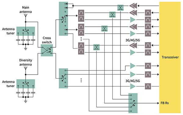 Figure 2: The use of an RF cross switch enables the selection of the best-performing antenna for uplinks or downlinks. (Image source: Infineon)
Diversity switches and LNAs
Sometimes, switching to the best antenna is still insufficient to support the required bandwidth. When that happens, an additional channel called the diversity path is added to the RF signal chain. Antenna diversity improves the quality and reliability of transmission and reception. Diversity switches are used in a range of applications, from Wi-Fi networking equipment to smartphones and tablet computers. These switches can be used to compensate for multipath interference in signal reception. The receiver monitors the incoming signals and switches between the antennas based on the relative signal strengths. As in the case of RF cross switches, diversity switches need to have high isolation, low insertion losses, and generate low harmonics.
LNAs are another key part of the RF signal chain (Figure 3). Like the various approaches to antenna management, the use of LNAs can improve reception quality and boost data rates. LNAs are available with a fixed gain or with multiple gain steps that can be used to fine-tune performance. LNAs based on monolithic microwave integrated circuit (MMIC) technology have traditionally been produced using gallium arsenide (GaAs) technology. More recently developed silicon germanium (SiGe) LNA MMICs can support the needed frequencies at a lower cost. LNAs are highly compact devices that can be readily integrated into very small packages. In addition, LNA MMICs are available with integrated protection from electrostatic discharge (ESD), and their low power consumption makes them well-suited for mobile devices and wearables where SWaP is an important consideration.
 Figure 3: The use of diversity switches and LNAs can help improve reception quality and boost data rates. (Image source: Infineon)
Control interfaces
Antenna tuning switches, cross switches, and diversity switches generally require an interface with the system controller. In simple implementations, a general-purpose input/output (GPIO) interface is often used. A GPIO is an uncommitted software controllable signal pin on an IC that can be programmed to act as an input or output, or both, as needed.
For more complex control needs, the mobile industry processor interface (MIPI) standard is generally used. The MIPI RF front-end (RFFE) control interface has been optimized for use in high-performance RF signal chains to provide fast, semi-automated, and extensive control functions. The MIPI RFFE can include up to 19 devices per bus (up to four leader devices and 15 follower devices). It’s designed for use with LNAs, antenna tuners, switches, power amplifiers, and filters. MIPI RFFE can facilitate the design, configuration, and integration of RF signal chains, and it supports the use of components from different suppliers.
MIPI controllable LNA
Designers can use the BGA9H1MN9E6329XTSA1 LNA from Infineon for high-performance RF signal chains. The MIPI interface can control the eight gain modes and the 11 bias modes to increase system dynamic range by actively accommodating changing conditions in the RF environment (Figure 4). It’s designed for use in the 3GPP bands between 1.4 and 2.7 gigahertz (GHz) (primarily for bands B1, B3, n41, and B21). It can provide a 0.6 decibel (dB) noise figure and up to 20.2 dB gain with 5.8 milliamperes (mA) of current. It operates with supply voltages from 1.1 to 2.0 volts and is qualified for industrial applications based on JEDEC47/20/22.
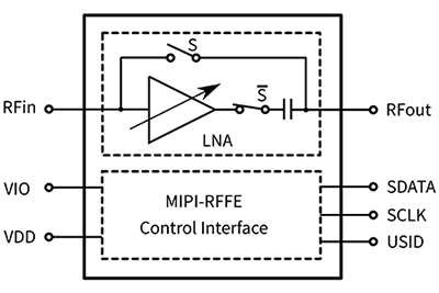 Figure 4: The MIPI interface on this LNA can control eight gain modes of operation and 11 bias modes for performance optimization. (Image source: Infineon)
It has several features that help to meet challenging SWaP requirements, including:
- Size: The nine-pin TSNP-9 measures 1.1 × 1.1 millimeters (mm), and its 0.375 mm height makes it well-suited for space-restricted applications.
- Weight: The TSNP-9 package has been optimized for use where light weight is a requirement.
- Power: The BGA9H1MN9E6329XTSA1 LNA has a bypass current of only 2 microamperes (µA), extending battery run times.
Antenna diversity switch
The BGS12WN6E6327XTSA1 wideband single pole double throw (SPDT) diversity switch from Infineon has a typical switching speed of 160 nanoseconds (ns), plus integrated control logic (decoder) and ESD protection (Figure 5). Designed for use in Wi-Fi, Bluetooth, and ultra-wideband RF signal chains, either of the two ports can connect to a diversity antenna and handle up to 26 dB, referenced to 1 milliwatt (dBm). It’s fabricated with MOS technology and provides the performance of a GaAs device, but eliminates the need for external DC blocking capacitors on the RF ports unless an external DC voltage is expected to be applied.
The chip includes CMOS logic driven by a single CMOS or TTL compatible control signal. It features high port-to-port isolation and low insertion losses up to 9 GHz. To reduce size and weight, the device comes in a PG-TSNP-6-10 package that measures 0.7 × 1.1 mm with a maximum height of 0.375 mm. It can operate with supply voltages up to 4.2 volts with a typical supply current of 36 µA and a control current of 2 nanoamperes (nA), maximizing run time in battery-powered devices.
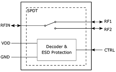 Figure 5: The BGS12WN6E6327XTSA1 SPDT diversity switch can switch in 160 ns and includes integrated control logic and ESD protection. (Image source: Infineon)
RF cross switch
Infineon’s BGSX22G6U10E6327XTSA1 RF CMOS cross switch is specifically designed for GSM, WCDMA, LTE, and 5G applications. This double-pole double-throw (DPDT) switch features low insertion loss at frequencies up to 7.125 GHz, low harmonic generation, and high isolation between its RF ports. Its switching time of 1.3 microseconds (µs) enables support of 5G sounding reference signal (SRS) applications. It has a GPIO control interface and operates with supply voltages from 1.6 to 3.6 volts. The PG-ULGA-10 package measures 1.1 × 1.5 mm, is 0.60 mm thick and is optimized for space and weight-constrained applications. This low-power device has a typical supply current of 25 µA and a control current of 2 nA.
Antenna tuning switch
Designs that require a single-pole four-throw (SP4T) antenna tuning switch optimized for applications up to 7.125 GHz can use Infineon’s BGSA14M2N10E6327XTSA1. The four 0.85 ohm (Ω) on-resistance ports are designed for use in high Q tuning applications. The MIPI RFEE digital control interface simplifies implementation in RF signal chains. Its peak voltage capability of 45 volts and low capacitance of 160 femtofarads (fF) in the OFF state make it well-suited for switching inductors and capacitors in RF antenna matching circuits without significant losses (Figure 6). The 1.3 × 0.95 mm, 0.375 mm high, TSNP-10-9 package combined with a 22 µA current consumption make this device capable of supporting challenging SWaP applications.
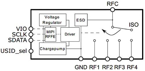 Figure 6: The BGSA14M2N10E6327XTSA1 can efficiently switch inductors and capacitors in RF antenna matching circuits. (Image source: Infineon)
RF transistors
A high-performance RF signal chain begins with the transceiver and RF amplifier section. This requires RF power transistors like the BFP760H6327XTSA1 wideband NPN RF heterojunction bipolar transistor (HBT) from Infineon that features:
- Low minimum noise figure (NFmin) of 0.95 dB at 5.5 GHz, 3 volts, 10 mA
- High maximum power gain (Gms) of 16.5 dB at 5.5 GHz, 3 volts, 30 mA
- High linearity with 3rd order intercept point at output (OIP3) of 27 dBm at 5.5 GHz, 3 volts, 30 mA
This power transistor is qualified for industrial applications. It’s designed for use in wireless and satellite communications systems, GPS navigation devices, mobile multimedia devices, and other high-performance RF applications.
TSNP package options
The small size of TSNP packages requires stable geometry tolerances on the pc board, and a non-solder mask defined (NSMD) pad design should be used. Pad tolerances for NSMD are lower compared with solder resist. For NSMD, traces on the pc board should be 100 micrometers (µm) or less. Typically, pc board pads for bottom-only TSNP, as used by the BGA9H1MN9E6329XTSA1 LNA, the BGS12WN6E6327XTSA1 antenna diversity switch, and the BGSA14M2N10E6327XTSA1 antenna tuning switch described above, are designed by transferring the package pad outline and adding 25 µm around the sides of the pads.
Designers need to be aware that there’s more than one style of TSNP pad. There’s the standard pad, and there are pads designed for optical lead tip inspection (LTI) (Figure 7). LTI devices require a larger mounting area since the pc board pad needs to extend beyond the package outline by a 400 μm minimum (Figure 7). While the LTI design supports optical inspection, it may not be suited for SWaP critical designs that require the smallest possible solution size.
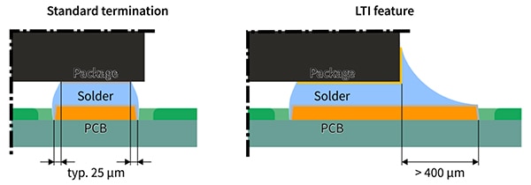 Figure 7: TSNP packages are available that use standard pads (left), or larger pads optimized for optical LTI (right). (Image source: Infineon)
Conclusion
SWaP considerations are important when specifying antenna tuners, RF cross switches, antenna diversity switches, LNAs, and low-noise RF transistors in a range of portable and wearable wireless devices. As shown, Infineon offers designers a range of devices for use in high-performance RF signal chain applications that can also satisfy demanding SWaP requirements. Using these devices, designers can optimize the reliability and bandwidth of the RF signal chain and extend battery life.
Recommended Reading

Disclaimer: The opinions, beliefs, and viewpoints expressed by the various authors and/or forum participants on this website do not necessarily reflect the opinions, beliefs, and viewpoints of DigiKey or official policies of DigiKey.


