How to Optimize for Isolation and Performance Using Advanced Digital Isolators
Contributed By DigiKey's North American Editors
2025-01-29
Executive Summary: Isolation is very important in electronic systems, especially sensor-based circuits. This article discusses how iCoupler digital isolators from Analog Devices provide high-speed, reliable, and safe isolation using transformer-based magnetic coupling technology with features like high isolation voltage, low power consumption, minimal propagation delay, and strong common-mode transient immunity, supported by evaluation tools for effective implementation. The iCoupler digital isolators core specifications, which include minimal degradation over time and temperature, also ensure high performance over the lifetime of the system.
Designers of electronic systems need to incorporate power and signal isolation to meet performance requirements while meeting regulatory mandates for user and device safety. The isolation of an AC power path is readily accomplished with a transformer. The isolation of a DC power rail also ultimately relies on a transformer, though it requires more circuitry. However, isolation for analog signals that have been digitized, as well as for digital serial data streams, presents different challenges and complications.
In this instance, the energy-transfer technique used for isolation must preserve signal integrity across the isolation barrier to maintain system performance. While there are many ways to implement isolation, designers must ensure signal integrity at higher data rates and in more challenging environments. Consequently, they increasingly turn to digital isolators that can transfer data at 150 megabits per second (Mbps).
This article briefly examines why isolation is required, emphasizing the need in sensor-based circuits. It then looks at various aspects of isolation using state-of-the-art digital isolators from Analog Devices and shows how they can be applied.
Isolation: why and where
There are multiple reasons why isolation is needed in sensor-based circuits:
- Isolation can eliminate common-mode voltage variations and minimize some types of electromagnetic interference (EMI). It ensures cleaner and more accurate measurements by preventing external noise sources from corrupting the acquired signal. It also allows measurement of small signals that have high common-mode voltages.
- Due to differences in potentials between circuit grounds, ground loops can introduce voltage differentials that distort the measured signal. Isolation breaks the ground loop.
- Isolation prevents hazardous voltage spikes, transients, or surges from reaching sensitive measurement components. This protects the measurement circuitry, any connected devices, and the user.
- Isolation supports safe level translation between different circuit functions. Circuitry on one side of the isolation barrier can be at the transducer voltage, while circuitry on the other side can be at 3.3 or 5 volts for logic-level signals.
For example, in a high-voltage battery stack, it is often necessary to know the individual cell voltages to ensure the system operates safely and achieves the longest possible battery life. The voltage across a single cell must be measured despite the presence of up to several hundred volts of common-mode voltage along the series-connected battery stack.
While it is possible to use analog circuitry and isolation amplifiers to overcome this problem, such approaches do not meet the need for measurements with higher bandwidth and resolution while maintaining system accuracy, linearity, and consistency.
Instead, the most accurate, economical, and efficient technique for performing these measurements is to isolate the entire measurement front-end, including the analog-to-digital converter (ADC), and then use an isolated serial link for the digitized data to the rest of the system (Figure 1).
 Figure 1: Using an isolated front-end when measuring the voltage of a single cell in a high-voltage stack overcomes the challenge of common-mode voltages. (Image source: Analog Devices)
This approach isolates the battery stack’s common-mode voltage while preventing any dangerous high voltages from migrating to the data-link side or the user in case of a fault.
Note that whenever there is a need for signal isolation, there is also a requirement to provide isolated power, as non-isolated power rails would contradict and negate the signal isolation. The needed power isolation can be implemented via a separate power isolation circuit or by using a battery as an independent and isolated power source.
How to provide isolation
Many parameters define isolation performance. Among these is the maximum voltage the isolation barrier can withstand before it fails. Regulations govern the required maximum, typically several thousand volts, depending on the application.
Several distinct technologies can be used to achieve isolation of digital signals. These include capacitive coupling, optical coupling (LED and phototransistor), RF transmission on a “micro” scale, and magnetic coupling.
The latter is a reliable technique with many positive attributes, but has historically required a relatively large and costly signal transformer. That situation changed with the introduction of iCoupler technology from Analog Devices. This approach uses chip-scale primary and secondary transformer coils separated by an isolation barrier created by layers of polyimide insulation (Figure 2). A high-frequency carrier transmits data across the isolation barrier to the secondary coil.
 Figure 2: iCoupler technology uses a high-frequency carrier to transmit data from the primary coil to the secondary coil across thick polyimide insulation. (Image source: Analog Devices)
In operation, the primary transformer is driven by a pulsed current through its primary coil to create a small, localized magnetic field that induces current in the secondary coil. The current pulses are short, at about 1 nanosecond (1 ns), so the average current is low to ensure low power consumption. Also, the on/off keying (OOK) technique used for pulsing and the differential architecture provide a very low propagation delay and high-speed capability.
The polymer materials used in iCoupler offer robust isolation, as the material is qualified in almost all applications. The most challenging use cases, such as medical devices and heavy industrial equipment, benefit most from this performance capability.
Polyimide also has lower stress than silicon dioxide (SiO2), an alternative barrier material, and can be increased in thickness as needed. In contrast, SiO2 thickness, and therefore isolation capability, is limited; stress on thicknesses greater than 15 micrometers (μm) may induce cracked wafers during processing, or delamination over the life of the isolator. Polyimide digital isolators use isolation layers as thick as 26 μm.
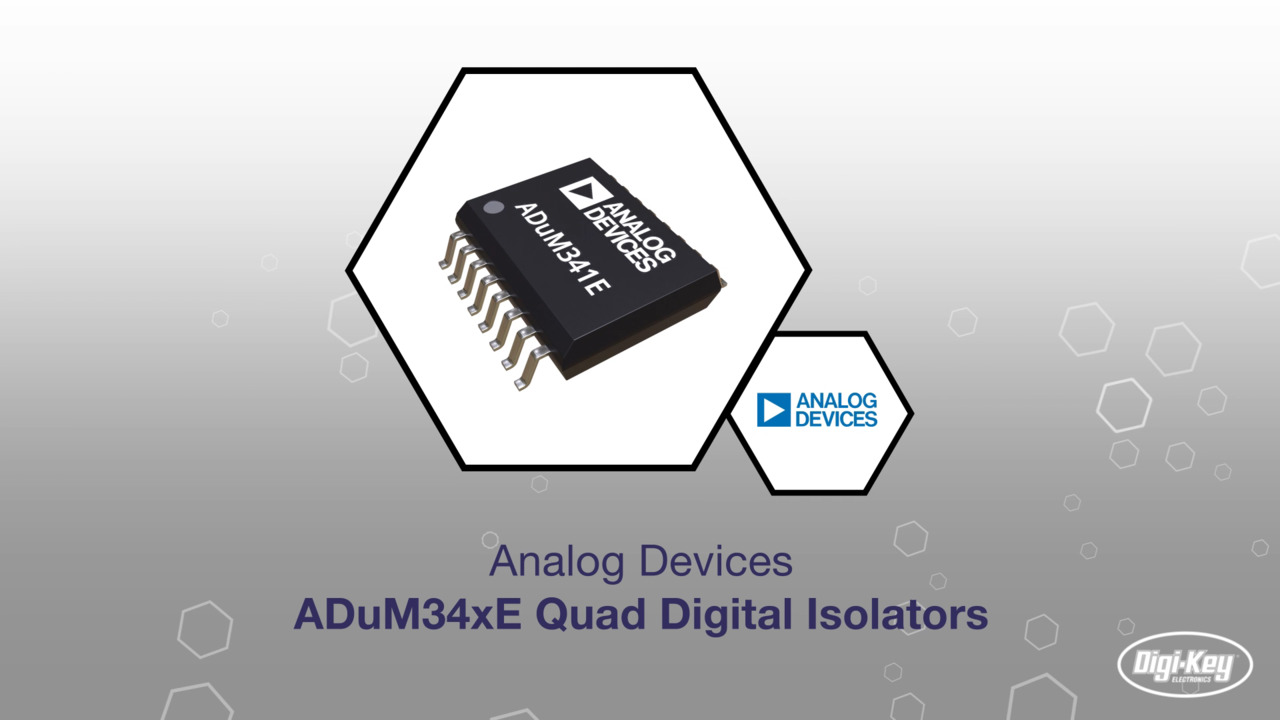
Analog Devices offers a variety of transformer-based iCoupler digital isolators. Among them are the ADUM340E0BRWZ-RL, ADUM341E0BRWZ-RL, and ADUM342E1WBRWZ 3000 volt rms, 150 Mbps isolators for CAN, RS-485, and SPI interfaces.
These three digital isolators are collectively called the ADuM34xE devices, differing primarily in their channel directionality. The ADuM340E has four forward channels, the ADuM341E has three forward and one reverse channel, and the ADuM3421 has two forward and two reverse channels (Figure 3).
") Figure 3: The three four-channel digital isolators in the ADuM34xE series have similar specifications but differ in channel directionality. (Image source: Analog Devices)
Figure 3: The three four-channel digital isolators in the ADuM34xE series have similar specifications but differ in channel directionality. (Image source: Analog Devices)
The three isolators are each offered with a choice between two fail-safe modes (Figure 4): the output state is set to low if the input side is off or not operating (low fail-safe), or the output state is set to high if the input side is off or not operating (high fail-safe). This allows the isolators to revert to a known state when used in critical applications.
") Figure 4: Shown are the operational block diagrams of a single channel of an ADuM34xE device illustrating the low fail-safe (top) and high fail-safe (bottom) options. (Image source: Analog Devices)
Figure 4: Shown are the operational block diagrams of a single channel of an ADuM34xE device illustrating the low fail-safe (top) and high fail-safe (bottom) options. (Image source: Analog Devices)
Note that there is no relationship between the input-side (VDD1 pin in Figure 3) and output-side (VDD2) supplies. They can simultaneously operate at any voltage within their specified operating ranges and sequence in any order. This feature enables the isolator to perform voltage translations of 2.5 V, 3.3 V, and 5 V logic, among others.
Nuances of ADuM34xE performance characteristics
The ADuM34xE isolators’ high isolation voltage, high speed, low power, and low propagation delay have direct applicability, but their architecture has more nuanced advantages that designers can use. For example, the aggregate power consumption scales with operating frequency, and the power requirements are roughly proportional to the speed at which the devices operate. Therefore, channels that are idle or that switch at very low speeds consume very little power. The result is a relative reduction in power consumption of one to two orders of magnitude compared to alternative isolation techniques.
Also, once the designer has determined the maximum serial clock rate for the application, the associated isolated power supply can be selected to provide enough current to support just this rate, eliminating the need to over-specify beyond the isolator’s maximum value.
Given the importance of timing and propagation delay in high-speed serial links, it is important to note that digital isolator performance does not degrade or shift over time and temperature. While jitter is less of an issue at low signaling rates where its error is small compared to the waveform period, at higher data rates, timing jitter becomes a significant percentage of the signal interval. Choosing an isolator with the lowest jitter can boost the isolated circuit’s signal-to-noise ratio (SNR) and efficiency.
Due to these characteristics of the iCoupler architecture, the device datasheets define guaranteed minimum and maximum power consumption, propagation delays, and pulse-distortion specifications over their entire operating temperature range of -40°C to +125°C. For designers, having these complete specifications simplifies calculations related to worst-case system performance.
With the digital isolators’ guaranteed numbers related to propagation delay (maximum of 10 ns) (Figure 5), skew, and channel-to-channel matching, the top-level system timing specifications can be modeled and evaluated as with other digital ICs.
 Figure 5: iCoupler technology results in a very low and fully characterized propagation delay of under 10 ns over the full operating temperature range. (Image source: Analog Devices)
Common-mode transient immunity (CMTI) is a lesser-known and easily overlooked specification. The constant switching in high-voltage applications such as electric vehicle (EV) and hybrid EV (HEV) charging circuitry, solar power systems, and motor drives introduces common-mode transients such as ringing and noise. The isolation technology in the ADuM34xE devices leverages a back-to-back center-tapped transformer architecture that provides a low-impedance path to ground for noise on each side of the isolation barrier. This allows them to achieve a CMTI rating of 100 kilovolts per microsecond (kV/µs) (minimum), significantly enhancing the integrity of the isolated signal.
Designers familiar with magnetics may be concerned that these isolators might be affected by magnetic interference that could corrupt the transmit pulses across the isolation barrier, causing errors. This concern is misplaced, as the transformers' small radius and air core mean an extremely large magnetic field or a very high frequency is required to induce a fault. Digital isolators are unaffected by 500 amperes (A) at 1 megahertz (MHz) in a wire just 5 millimeters (mm) from the device.
Evaluating digital isolators
While the functionality of these isolators is straightforward, applying them requires attention to details, such as board layout, to ensure their high-voltage isolation capabilities and high-speed operation are not compromised.
To assist designers in using and evaluating the devices, Analog Devices offers the EVAL-ADUM34XEEBZ iCoupler Digital Isolator Interface Evaluation Board (Figure 6). This board has locations and layouts for one of each of the isolators, plus a fourth uncommitted location. The board features v-shaped grooves between each component (U1 to U4) to allow users to split the board into sections and examine a specific device on a breadboard or similar test fixture.
 Figure 6: The EVAL-ADuM34XEEBZ evaluation board supports all three ADuM34xE devices and has an open location for a user’s pinout-compatible device choice. (Image source: Analog Devices)
The EVAL-ADuM34XEEBZ board follows appropriate printed circuit board (pc board) design practices, including a ground plane on each side of the isolation barrier. iCoupler device evaluation using this board requires only an oscilloscope, a signal generator, and a 2.25 V to 5.5 V power supply.
Conclusion
Isolation is needed in many designs to maintain signal integrity, ensure user and device safety, and meet regulatory mandates. Digital isolation devices based on iCoupler magnetic coupling technology from Analog Devices offer an easy-to-use and reliable high-speed solution. Their core specifications, including minimal degradation over time and temperature, ensure superior long-term performance.
Disclaimer: The opinions, beliefs, and viewpoints expressed by the various authors and/or forum participants on this website do not necessarily reflect the opinions, beliefs, and viewpoints of DigiKey or official policies of DigiKey.