How to Improve Ultrasound System Image Quality Using Ultra-Low-Noise Supplies
Contributed By DigiKey's North American Editors
2023-02-09
Ultrasound technology, a widely used noninvasive tool in medical diagnostics and other applications, has shifted from static to dynamic images, and from black-and-white presentation to color Doppler images. These important enhancements are largely due to the introduction of digital ultrasound technology. While these advances have increased the effectiveness and versatility of ultrasound imaging, it is equally important for these systems to offer improved image quality via advances in the head-end ultrasound probe, and the analog front-end (AFE) that drives the probe and captures the return signals.
One of the impediments to achieving this improved image quality is noise, so the design goal is to increase the signal-to-noise ratio (SNR) of the system. This can be achieved in part by addressing noise due to the various power supply rails in the system. Note that such noise is not a single, simple entity. Instead, it has various characteristics and attributes which determine how it ultimately impacts system performance.
This article will look at the basic principle of ultrasound imaging, and then focus on different factors that affect image quality, primarily noise from the power supplies. It will use DC-DC regulator devices from Analog Devices as examples of power supply components that can greatly improve SNR and other aspects of ultrasound system performance.
Basics of ultrasound imaging
The concept is simple: generate a sharp acoustic pulse, then “listen” for its echo reflection as it encounters obstacles or various interfaces between organs and their differing acoustic impedances. By doing these impulse-return sequences repeatedly, the reflections can be used to create an image of the reflecting surfaces.
For most modes of ultrasound, the array of piezoelectric transducers sends a limited number of wave cycles (typically two to four) as a pulse. The frequency of these waves in each cycle is usually in the range of 2.5 to 14 megahertz (MHz). The array is controlled via beamforming techniques analogous to a phased-array RF antenna, so the overall ultrasound pulse can be focused and steered to create a scan. The transducer then switches to receive mode to sense the return of the reflected waves from within the body.
Note that the transmit/receive timing ratio is typically about 1%/99%, with a pulse repetition frequency usually between 1 and 10 kilohertz (kHz). By timing the pulse from its transmission to received echoes and knowing the speed at which the ultrasound energy propagates through body tissue, it is possible to calculate the distance from the transducer to the organ or interface reflecting the wave. The amplitude of the returning waves determines the brightness of the pixels assigned to the reflection in the ultrasound image, after considerable digital post-processing.
Understanding system requirements
Despite the conceptual simplicity of the underlying principle, a complete, high-end ultrasound imaging system is a complicated device (Figure 1). The ultimate performance of the system is largely determined by the transducer and analog front-end (AFE), while post-processing of the digitized reflected signal allows algorithms to enhance the situation.
Not surprisingly, system noise of various types is one of the limiting factors in image quality and performance, again analogous to the consideration of bit error rate (BER) versus SNR in digital communication systems.
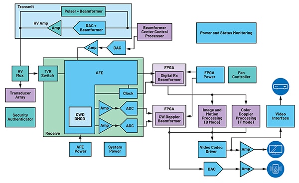 Figure 1: A complete ultrasound imaging system is a complex combination of a significant amount of analog, digital, power, and processing functionality; the AFE defines the bounds of system performance. (Image source: Analog Devices)
There is a transmit/receive (T/R) switch between the piezoelectric transducer array and the active electronics. The role of this switch is to prevent the high-voltage transmit signals driving the transducer from reaching and damaging the low-voltage receive-side AFE. After the reflection received is amplified and conditioned, it is passed to the analog-to-digital converter (ADC) of the AFE, where it is digitized and undergoes software-based image processing and enhancement.
Each of the different imaging modes of an ultrasound system has different requirements for the dynamic range—and thus SNR—or noise requirements:
- For black-and-white image mode, a dynamic range of 70 decibels (dB) is required; the noise floor is important as it impacts the maximum depth at which the smallest ultrasound echo can be seen in the far field. This is called penetration, one of the key features of black-and-white mode.
- For pulse wave doppler (PWD) mode, a 130 dB dynamic range is required.
- For continuous wave doppler (CWD) mode, 160 dB is needed. Note that the 1/f noise is particularly important for the PWD and CWD modes, as both of those images include the low-frequency spectrum element below 1 kHz, and the phase noise impacts the Doppler frequency spectrum higher than 1 kHz.
These requirements are not easy to meet. As the ultrasound transducer frequency is typically from 1 MHz to 15 MHz, it will be affected by any switching frequency noise within this range. If there are intermodulation frequencies within the PWD and CWD spectrums (from 100 Hz to 200 kHz), the obvious noise spectrums will appear in the Doppler images, which is unacceptable in the ultrasound system. For maximum system performance and image quality (clarity, dynamic range, lack of image speckling, and other figures of merit), it’s important to look at sources which cause loss of signal quality and degradation of SNR.
The first one is obvious: due to attenuation, the returns from tissues and organs deeper in the body (such as kidneys) are far weaker than those from those close to the transducer. Therefore, the reflected signal is “gained up” by the AFE so that it occupies as much of the AFE’s input range as possible. For this, an automatic gain control (AGC) function is used. This AGC function is similar to the one used in wireless systems where the AGC assesses wireless RF received signal strength (RSS) and dynamically compensates for its random, unpredictable changes over a span of tens of decibels.
However, the situation is different in the ultrasound application than it is for a wireless link. Instead, the path attenuation is known approximately, as is the velocity of acoustic energy propagation velocity—1540 meters per second (m/s) in soft tissue, or about five times faster than propagation in air at about 330 m/s—and so the attenuation rate is also known.
Based on this knowledge, the AFE uses a variable-gain amplifier (VGA) which is arranged as a time-gain compensation (TGC) amplifier. The gain of this VGA is linear-in-dB and is configured such that a linear-versus-time ramping control voltage increases the gain-versus-time to compensate to a large extent for the attenuation. This maximizes SNR and the use of the dynamic range of the AFE.
Noise types and how to address them
Although in-body and patient-induced signal noise is beyond the control of the ultrasound system designer, internal system noise must be managed and controlled. For this, it’s important to understand the noise types, their impact, and what can be done to reduce them. The primary areas of concern are switching regulator noise; white noise due to the signal chain, clock, and power; and layout related noise.
- Switching regulator noise: Most switching regulators use a simple resistor to set the switching frequency. The unavoidable tolerance of the nominal value of this resistor introduces different switching frequencies and harmonics as the frequencies of different independent regulators mix and cross-modulate each other. Consider that even a tight-tolerance resistor with a 1% inaccuracy results in a 4 kHz harmonic frequency in a 400 kHz DC-DC regulator, making the harmonics harder to control.
A better solution is to select a switching regulator IC with a synchronization feature implemented via a SYNC connection on one of its package pins. Using this feature, an external clock can distribute a signal to the various regulators so that they all switch at the same frequency and phase. This eliminates the mixing of the nominal frequencies and associated harmonic products.
For example, the LT8620 is a high-efficiency, high-speed synchronous monolithic step-down switching regulator that accepts a wide input voltage range up to 65 volts, and consumes only 2.5 microamperes (μA) of quiescent current (Figure 2). Its low ripple “Burst Mode” operation enables high efficiency down to very low output currents while keeping the output ripple below 10 millivolts (mV) peak-to-peak. A SYNC pin allows for user-established synchronization to an external clock from 200 kHz to 2.2 MHz.
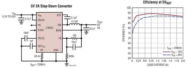 Figure 2: The highly efficient LT8620 step-down switching regulator includes a SYNC pin so its clocking can be synchronized with other system clocks, minimizing clock intermodulation effects. (Image source: Analog Devices)
Another technique is to use a switching regulator that employs random spread-spectrum clocking to spread the generated electromagnetic interference (EMI) across a wider band, lowering its peak value at any specific frequency. While this is an attractive solution for some applications that are less SNR critical and more concerned with meeting EMI requirements, it introduces uncertainties in the resultant harmonics that will be created across a wider spectrum, making them harder to control. For example, a switching frequency spread of 20% for EMI consideration results in harmonic frequencies between zero and 80 kHz in a 400 kHz power supply. Thus, while this approach to lowering EMI “spikes” may help meet relevant regulatory mandates, it may be counterproductive for the special SNR needs of ultrasound designs.
Switching regulators with constant frequency help avoid this issue. ADI’s family of Silent Switcher voltage regulators and μModule regulators feature constant-frequency switching. At the same time, they offer EMI performance with selectable spread spectrum techniques, to provide excellent transient response without introducing the uncertainties associated with spread spectrum.
The Silent Switcher regulator family is not limited solely to lower power regulators, either. For example, the LTM8053 is a 40 VIN (maximum), 3.5 A continuous, 6 A peak, step-down regulator that includes a switching controller, power switches, an inductor, and all support components. Only input and output filter capacitors are needed to finish the design (Figure 3). It supports an output voltage range from 0.97 to 15 volts, and a switching frequency range of 200 kHz to 3 MHz, each set by a single resistor.
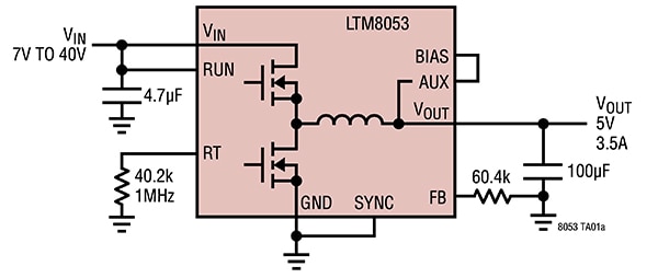 Figure 3: The LTM8053 member of the Silent Switcher family can deliver 3.5 A continuous/6 A peak current; it accepts an input of 3.4 to 40 volts and can provide output across a wide 0.97-to-15-volt range. (Image source: Analog Devices)
The LTM8053’s unique packing helps maintain low EMI along with higher current output. A copper pillar flip-chip package in a Silent Switcher µModule regulator helps to reduce parasitic inductance and optimize spike and dead time, enabling high-density design and large current capability in a small package (Figure 4). If more current is needed, multiple LT8053 devices can be connected in parallel.
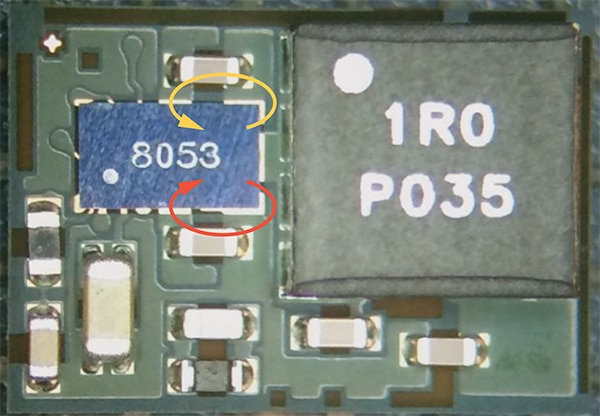 Figure 4: The LTM8053 (and other Silent Switcher devices) integrate a copper pillar flip-chip, enabling high-density design and large current capability in a small package while minimizing parasitic inductance. (Image source: Analog Devices)
The Silent Switcher line’s technology and topology are not limited to single-output regulators. The LTM8060 is a quad-channel, 40 VIN Silent Switcher μModule regulator with a configurable 3 A output array (Figure 5). It operates up to 3 MHz and is packaged in a compact (11.9 mm × 16 mm × 3.32 mm), over-molded ball grid array (BGA).
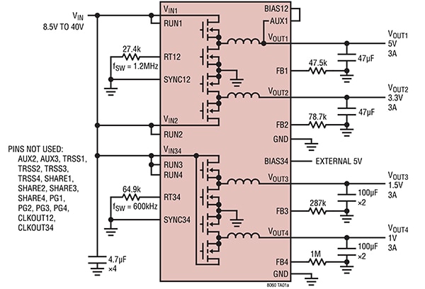 Figure 5: The LTM8060 is a four-channel μModule configurable array with 3 A/channel output in a compact package measuring just 11.9 mm × 16 mm × 3.32 mm. (Image source: Analog Devices)
One of the interesting aspects of this quad-channel device is that its outputs can be paralleled in different configurations to match different load-current needs, up to a maximum of 12 A (Figure 6).
 Figure 6: The four 3 A outputs of the LTM8060 can be arranged in different parallel configurations to match the application’s DC rail requirements. (Image source: Analog Devices)
In summary, the Silent Switcher regulators offer many benefits with respect to noise, harmonics, and thermal performance (Figure 7).
|
Figure 7: Shown are the key attributes of the Silent Switcher family of regulators relative to important design perspectives. (Image source: Analog Devices)
- White noise: There are also many white noise sources in an ultrasound system, which leads to background noise and image “speckles.” This noise comes primarily from the signal chain, clock, and power. Adding a low-dropout (LDO) regulator at the power pin of a sensitive analog component can resolve this.
ADI’s next-generation LDO regulators, such as the LT3045, feature an ultra-low noise level of around 1 microvolt (μV) rms (10 Hz to 100 kHz), and provide a current output of up to 500 mA at a typical dropout voltage of 260 mV (Figure 8). Operating quiescent current is nominally 2.3 mA and drops to much lower than 1 μA in shutdown mode. Other low-noise LDOs are available to cover current from 200 mA to 3 A.
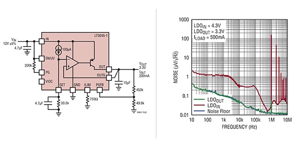 Figure 8: The LT3045 LDO regulators are noted for their ultra-low noise of around 1 μV rms over a current range from 200 mA to 3 A. (Image source: Analog Devices)
- Board Layout: In most pc board layouts, there is a conflict between high-current signal traces from the switching power supplies and the adjacent low-level signal traces, as noise from the former can couple into the latter. This switching noise is usually generated by the “hot loop” created by the input capacitor, top-side MOSFET, bottom-side MOSFET, and parasitic inductances due to wiring, routing, and bonding.
The standard solution is to add a snubber circuit to reduce electromagnetic emission, but this decreases efficiency. The Silent Switcher architecture improves performance and maintains high efficiency even at a high switching frequency by creating an opposite hot loop (called “splitting”) using bidirectional emissions, reducing EMI by about 20 dB (Figure 9).
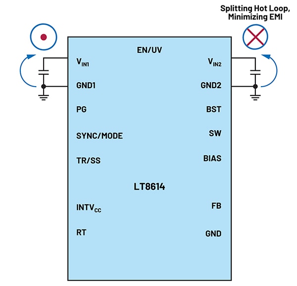 Figure 9: By establishing an opposing “hot loop” that splits the current-flow path, the Silent Switcher significantly cuts EMI by about 20 dB. (Image source: Analog Devices)
Efficiency versus noise
It may seem that if there is a tradeoff between power supply noise versus potential efficiency, the need for ultra-low noise in the ultrasound application should prevail. After all, a few more milliwatts of dissipation should not be that much of a burden at the “big-picture” system level. Further, why not increase the energy pulsed by the transducer to increase the pulse signal strength and thus the reflected SNR?
But this tradeoff has another complication: self-heating in the handheld digital probe that contains the transducer, piezoelectric element driver, AFE, and other electronic circuitry. Some of the probe’s electrical energy is dissipated in the piezoelectric element, lens, and backing material, thus causing transducer heating. Along with wasted acoustic energy in the transducer head, this will result in heating and a temperature rise at the probe.
There is a limit on the maximum allowable transducer surface temperature. IEC standard 60601-2-37 (Rev 2007) restricts this temperature to 50°C when the transducer is transmitting into air, and 43°C when transmitting into a suitable phantom (a standard body simulator); the latter limit implies that skin (typically at 33°C) can be heated by 10°C at most. Thus, transducer heating is a significant design consideration in complex transducers. These temperature limits may effectively restrict the acoustic output that can be employed, independent of available DC power.
Conclusion
Ultrasound imaging is a widely used, invaluable, noninvasive, and risk-free medical imaging tool. Although the basic principle is conceptually simple, designing an effective imaging system requires a significant amount of complex circuitry, along with multiple DC regulators to power its various subcircuits. These regulators and associated power must be efficient, but also be very low noise due to the extreme SNR and dynamic range mandates on the reflected acoustic signal energy. As shown, LDOs and Silent Switcher ICs from Analog Devices meet these requirements without compromising space, EMI, or other key attributes.
Related Content
- Maxim/Analog Devices, Tutorial 4696, “Overview of Ultrasound Imaging Systems and the Electrical Components Required for Main Subfunctions”
- Analog Devices, “Silent Switcher™ Technology by Analog Devices” (video)
- Analog Devices, “Low Noise Silent Switcher μModule and LDO Regulators Improve Ultrasound Noise and Image Quality”
- Analog Devices, “Silent Switcher Devices Are Quiet and Simple”

Disclaimer: The opinions, beliefs, and viewpoints expressed by the various authors and/or forum participants on this website do not necessarily reflect the opinions, beliefs, and viewpoints of DigiKey or official policies of DigiKey.


