Bluetooth 4.1, 4.2 and 5 Compatible Bluetooth Low Energy SoCs and Tools Meet IoT Challenges (Part 2)
Contributed By DigiKey's North American Editors
2017-04-20
Editor’s Note: Significant upgrades to Bluetooth low energy introduced through versions 4.1, 4.2 and 5 were designed to make the short-range wireless standard a better choice for Internet of things (IoT) wireless applications. Part 1 of this two-part series describes those upgrades and outlines their advantages. Part 2, here, introduces Bluetooth low energy SoCs, modules and kits, and discusses their relative tradeoffs as a design approach. By the end of the series, a competent designer should be comfortable starting a Bluetooth low energy design.
While several chip vendors now supply Bluetooth low energy transceiver systems-on-chip (SoCs) that comply with the latest version of the standards, taking advantage of all the new functionality is tricky. If starting from a blank sheet, the developer must cope with relatively complex RF peripheral circuit design and then write application software that optimizes their application, yet interfaces smoothly with manufacturers’ tested and verified Bluetooth low energy protocol software (“stack”). Then they must gain regulatory compliance for their wireless prototype. Opting for a module can ease the process by eliminating the peripheral circuit design and compliance testing, but this can increase both the cost and solution footprint.
Using examples of commercial Bluetooth low energy chips and modules, stacks, open-source application software, reference designs and vendor supplied developments tools, this article describes how engineers with limited RF design expertise can address the various challenges and take optimal advantage of the benefits that wireless connectivity brings.
Hardware design
Part 1 of this article described how silicon vendors have generally adopted a highly integrated SoC approach for their Bluetooth low energy products. The SoCs are almost exclusively based on 2.4 GHz radios, supervised by ARM Cortex-M0, M3 or M4F embedded processors with flash and RAM to store the stack firmware and application software. Other on-chip resources typically include power management, a selection of peripherals and I/O such as pulse width modulation (PWM), analog-to-digital conversion (ADC), and a universal asynchronous receiver/transmitter (UART).
In conjunction with introducing single-chip hardware, silicon vendors are working to make it much easier for non-expert RF engineers to design wireless products by supplying reference designs, application notes and design tools. Some RF knowledge is an advantage, of course, but it is possible for an inexperienced engineer to design and develop a fully functioning wireless product.
Cypress Semiconductor’s CYBL1xx7x Bluetooth 4.2 transceiver SoC, design tools and documentation are a good example of this full solution approach by vendors. Cypress’ SoC comprises five subsystems integrated into a single IC. This eliminates many of the peripheral components that were previously required for a Bluetooth low energy solution. (Figure 1).

Figure 1: Bluetooth low energy chipmakers generally take a highly integrated SoC approach. The solutions require few peripheral components and use ARM Cortex-M[x] processors to run both the stack and application code. The schematic shows Cypress Semiconductor’s CYBL1xx7x Bluetooth low energy SoC. (Image source: Cypress Semiconductor)
Chief among these subsystems is the CPU subsystem, typically comprising an embedded ARM processor and memory blocks. A direct memory access (DMA) controller enables certain operations to take place without using MCU resources. The embedded ARM core brings many advantages. These include wide adoption, a strong ecosystem, and the support of several popular integrated design environments (IDEs). The core has been specifically designed for low-power consumption and the device has sufficient computational overhead to concurrently run the stack and sophisticated application code. This eliminates the complexity, cost and space requirements of a separate application processor.
The CYBL1xx7x’s Bluetooth low energy subsystem consists of the link layer (LL) engine and physical layer (PHY). (See Part 1 of this article for more detail about the stack.) The LL engine supports both Bluetooth Central and Peripheral roles. The RF transceiver incorporates an integrated balun, which serves as a single-ended RF port pin to drive a 50 Ω antenna terminal through a matching network (see below). The output power is programmable from –18 dBm to +3 dBm to suit the application.
The other subsystems of the Cypress SoC include system resources such as power management and clock control, peripherals and I/O. Peripherals and I/O have largely been selected to match the typical sensor applications of Bluetooth low energy SoCs.
While a SoC like the Cypress CYBL1xx7x incorporates all the hardware (and firmware) for a complete Bluetooth low energy solution, simply soldering the chip to a pc board and applying power is unlikely to result in a working solution. Like all RF designs, a functioning system requires additional circuitry in the form of passive components that create matching circuits (Figure 2).
")
Figure 2: Many Bluetooth low energy SoCs are highly integrated, minimizing the number of external components required for good operation as shown in this application circuit for Texas Instruments’ CC2640 SoC. However, the design of external circuitry is still tricky and referral to makers’ reference designs is advised. (Image source: Texas Instruments)
The key parameter that determines a good RF circuit from a poor one is its impedance (Z). At high frequencies, such as with a 2.4 GHz radio, the impedance at a given point on an RF trace is related to the characteristic impedance of that trace (Z0), which in turn depends on the pc board substrate, dimensions of the trace, its distance from the load, and the load’s impedance.
It turns out that when the load impedance (ZL), which for a transmitting system will be the antenna and for a receiving system is the Bluetooth low energy SoC, is equal to Z0, the measured impedance (Z) remains the same at any distance along the trace from the load. As a result, line losses are minimized and maximum power is transferred from transmitter to the antenna. Given this characteristic, it’s common practice to use a matching network designed to ensure an RF device’s impedance is equal to the trace’s characteristic impedance.
The performance of Bluetooth low energy SoCs is optimized by the vendor, based on the assumption that the traces to which the chip will be attached have a 50 Ω characteristic impedance. To achieve this, the SoCs integrate a balun with a nominal 50 Ω impedance. However, tuning with an external circuit is typically required to ensure the SoC’s impedance is precisely 50 Ω. Tuning is achieved using a circuit comprising a shunt inductor and series capacitor (or vice versa, depending on the measured value of the impedance before compensation).
The type of antenna depends on the application: for example, a Bluetooth low energy application such as a wireless mouse, requires a relatively short RF range and bandwidth. In this case, a common solution is to use a meandered inverted-F antenna (MIFA). A MIFA is formed using a pc board trace. It has a small footprint, is inexpensive and offers moderate gain (Figure 3).
However, a remote control with a voice recognition application requires greater range and bandwidth, making a wire antenna a better option. This offers greater range and gain than a MIFA, with the trade-offs of cost and space.

Figure 3: A MIFA antenna is a common solution for Bluetooth low energy applications because it can be formed using a pc board trace, occupies little area, is inexpensive and offers moderate gain. (Image source: Cypress Semiconductor)
Most Bluetooth low energy SoCs incorporate a resistor-capacitor (RC) circuit to provide a 16 or 32 kHz signal for timing purposes. This is a cost- and power-efficient option. If greater timing precision is needed, an external 32.768 kHz crystal oscillator (XTAL) must be added. In addition, an external high-frequency 16 or 32 MHz XTAL is typically required to provide a reference frequency and system clock.
Module advantages
There are some advantages to designing a Bluetooth low energy circuit using discrete components, notably lower bill-of-material (BoM) costs and real estate savings. However, it’s easy to get things wrong, which not only compromises the performance of the product, but also makes passing regulatory compliance challenging.
Fortunately, help is at hand in the form of reference designs from the Bluetooth low energy SoC makers. These target many common applications, ranging from wearables to remote controls and beacons. Adhering to a reference design is a good way to gain reasonable performance for a first prototype, making it much easier to optimize for the specific application.
An alternative is to turn to one of the many third-party modules. The advantages of doing so are many. The devices generally take advantage of the same Bluetooth low energy SoCs around which discrete designs are based, external components and circuitry have been optimised for performance, and perhaps most importantly, in most cases the module will already be certified to Bluetooth SIG and (for example) FCC regulations. The downsides are also plentiful. Greater expense (depending on volume), larger size, reliance on a single vendor and its ability to ship in volume, and (sometimes) a reduced number of accessible pins relative to the SoC upon which the module is based.
Modules are generally supported by a selection of development tools. u-blox's NINA-B111 Bluetooth 4.2 transceiver module is a good example of what’s available. The module is based on a Nordic Semiconductor nRF52832 SoC and is fully compatible with Bluetooth 4.2. In addition to the Nordic SoC, the module is fitted with an internal antenna (or an external antenna via a dedicated pin) and includes both 32 MHz and 32.786 kHz crystals (Figure 4). The range is specified to be more than 300 meters and the module is globally certified for Bluetooth SIG and international RF compliance. The NINA-B111 comes in a package measuring 10 x 14 mm (for the version with the internal antenna).

Figure 4: u-blox’s NINA-B111/2 is a tested and verified Bluetooth low energy module that requires no hardware development and offers several routes to ease software development. (Diagram drawn using DigiKey Scheme-it®. Original source image from u-blox)
The NINA-B111 (and similar modules based on Bluetooth low energy SoCs) allow engineers with little or no RF hardware expertise to work with fully verified hardware and RF protocol stack. This lets them concentrate on the application software to differentiate their product.
The RF protocol stack is typically pre-programmed into the SoC. Flash memory is often used to store the stack as it can be updated in the factory or in the field as the Bluetooth low energy specification evolves. Using this methodology, no customer resource needs to be allocated to stack development. With the stack taken care of, the next step is application code development.
Bluetooth application code development
There are two routes to developing successful application code. In the first instance the Bluetooth SIG encourages development and adoption of ‘Profiles’. These are software applications that customize the Bluetooth low energy product for a specific purpose, such as a human interface device (HID). The software defines the general behavior of devices running the same profile, how they communicate, and what kind of data is exchanged. Profiles also typically contain information such as dependencies on other profiles and suggested user interface formats. Along with HIDs, there are dozens of profiles available for applications as diverse as health & fitness monitoring, environmental sensing, and phone status alerts. Designers have a choice of using the Bluetooth low energy adopted profiles, or using the Generic Attribute Profile (GATT) to create their own.
However, even with a wide range of profiles and the option to create custom profiles, there’s always a chance there isn’t a good fit for the developer’s intended application. In this case, application software can be coded on development kits (DKs) and software DKs (SDKs) from the SoC makers or third parties such as ARM.
One complexity that can catch the unwary arises when integrating the application software with the RF protocol stack. Without due care, the elegant Bluetooth low energy firmware can be corrupted during compilation by the application code. This can greatly extend the debugging process.
Some vendors have addressed this challenge. For example, the u-blox NINA-B111 takes advantage of Nordic’s split software architecture on its nRF52832 SoC. Nordic’s stacks are known as “SoftDevices” and are delivered as tested and verified binary files that remain separate from the developer’s application code. The advantage is that the engineer doesn’t have to worry about corrupting the stack during development. The company’s DKs and SDKs look after interfacing the application code to the RF protocol stack during compilation.
For simple applications, the NINA-B111 is ‘pre-flashed’ with u-blox’s own connectivity software, enabling access to the company’s Low Energy Serial Port Service (SPS). By using the company’s free s-center software, the module can be configured using AT commands over the device’s UART interface (Listing 1).
Set up Central (Device A)
Enable Central Role: AT+UBTLE=1Default peer to Serial Port Service and always connected (use the address of Device B): AT+UDDRP=0 , sps://112233445566 , 2Startup NINA-B1 in data mode: AT+UMSM=1Store configuration: AT&WRestart NINA-B1: AT+CPWROFF
Set up Peripheral (Device B) (SPS is enabled by default)
Startup in data mode: AT+UMSM=1Store configuration: AT&WRestart: AT+CPWROFF
Listing 1. This code example shows how simple it is to connect two u-blox modules via SPS with one in a Central role and the other in a Peripheral role. (Code source: u-blox s center)
The NINA-B111 can also support complex applications such as lighting, asset tracking and metering. There are three design tools that support this more challenging application software development. The first is Nordic’s nRF5 SDK which includes a broad selection of drivers, libraries, and example applications. The second is the ability to develop application code in the open-source ARM mbed operating system (OS). mbed OS includes all the features required to design a connected product, including security, connectivity, an RTOS, and drivers for sensors and I/O devices. The third is a licensed software pack from a supplier such as Wirepas. If the modules are designed for large-scale mesh network applications, they can be configured using the software stack (Figure 5).

Figure 5: NINA-B111 software architecture exploits Nordic’s separated RF protocol stack and application code (left). This separation prevents stack corruption during application development and compilation. The Nordic SoftDevice (the stack) and u-blox connectivity software are pre-flashed into the module. Nordic, ARM and Wirepas mesh development tools can be used to build more complex applications. (Image source: u-blox)
Taking advantage of Bluetooth 5
Part 1 of this article described the range, throughput and other enhancements introduced with Bluetooth 5. Some commercial chips that support the new version are now coming on to the market. Texas Instruments’ CC2640R2F SimpleLink Bluetooth low energy SoC is among these devices and is supported by a range of development tools.
A bonus is that the CC2640R2F is part of TI’s SimpleLink microcontroller platform and hence shares a common development environment with other SimpleLink MCU-controlled wireless (and non-wireless) chips. Such an arrangement allows for wireless application code reuse even though it may have to be adapted for Bluetooth low energy applications.
TI’s key design tool for the CC2640R2 is a LaunchPad DK. This features more flash memory than its predecessors for the application code and supports programming and debugging from the Code Composer Studio and IAR Embedded Workbench IDEs.
Start development by downloading its Bluetooth low energy stack and then getting familiar with the DK by playing around with the Bluetooth low energy peripheral application. The application features sample code that demonstrates control of the LaunchPad DK’s LEDs from the TI SimpleLink SensorTag kit iOS app, or any compatible device supporting Bluetooth low energy connectivity. The project also demonstrates the flexibility of the stack and uses the DK’s onboard USB serial port to display diagnostic information about the Bluetooth low energy connection.
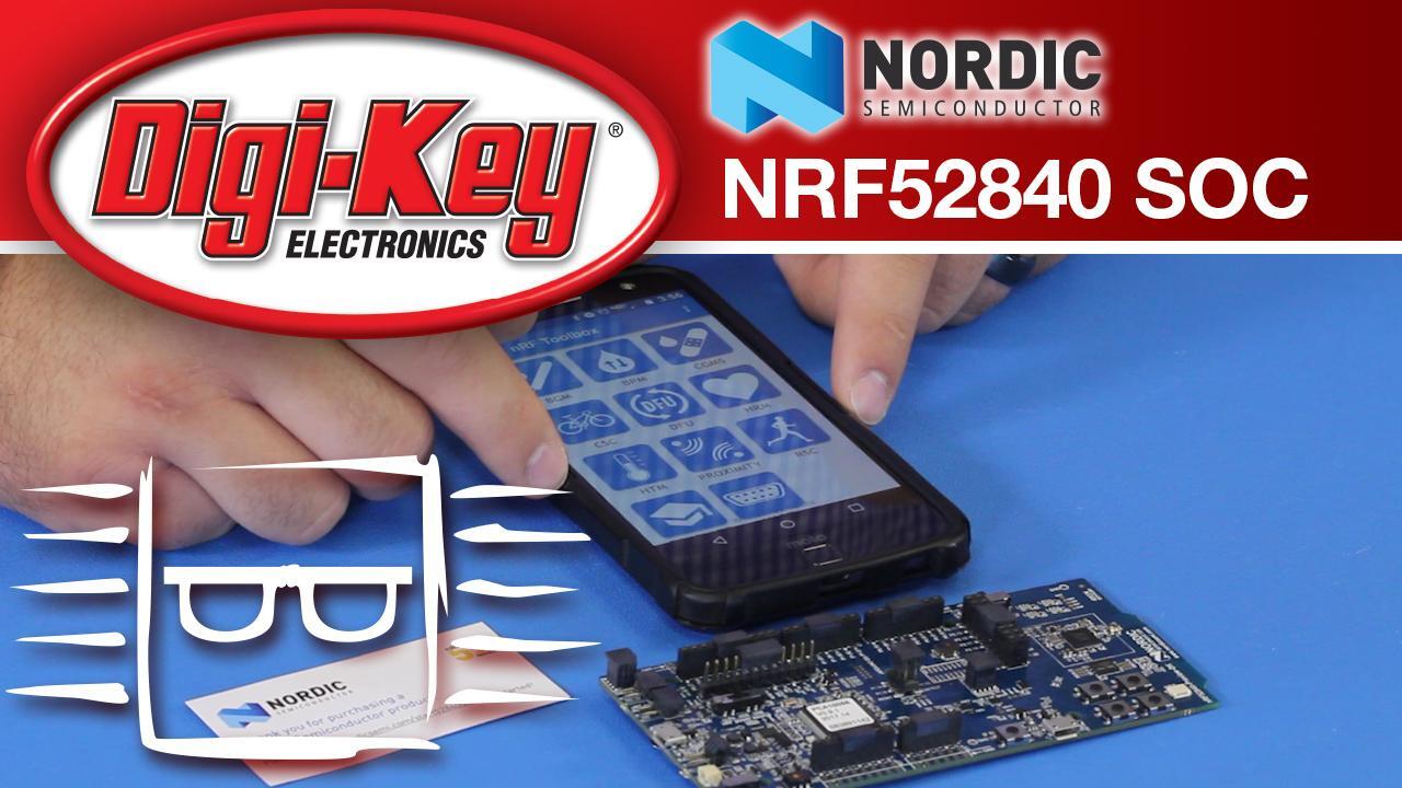
Nordic Semiconductor is another vendor that has announced a Bluetooth 5-compatible BLE SoC. The nRF52840 (currently only sampling) is based on an ARM® Cortex®-M4F processor and a re-engineered Bluetooth low energy radio. The flash and RAM have been increased to 1 Mbyte and 256 Kbytes respectively, relative to the nRF52832 described above. While full production of the nRF52840 is slated for mid-2017, a Preview DK (PDK) is on sale for developers who want to explore the chip’s capabilities and start writing application code (Figure 6).

Figure 6: Nordic Semiconductor’s nRF52840 PDK (together with an nRF SDK) allows developers to explore Bluetooth 5’s range and throughput enhancements by reconfiguring Bluetooth low energy parameters. (Image source: Nordic Semiconductor)
The PDK includes hardware, firmware source code, documentation, hardware schematics, and layout files. The DK is based around the nRF52840 SoC and is ARM mbed enabled. It includes buttons and LEDs for user interaction, USB, flash, and drag-and-drop mass storage device programming. Nordic also makes available the source code of the examples included with the DK and code libraries for application development.
By using two nRF52840 PDKs and Nordic’s nRF SDK (13.0.0-1.alpha) running the ATT_MTU Throughput Example, developers can configure various Bluetooth low energy parameters such as Maximum Transmission Unit (MTU), connection interval, Data Length Extension and the PHY data rate to test out their impact on throughput and range. In this way they can get familiar with the key enhancements of Bluetooth 5.
Conclusion
Part 1 of this article described the enhancements to the Bluetooth Core Specification introduced with Bluetooth 4.1, 4.2 and 5 that have made the technology practical for a wide range of Internet of things (IoT) applications. These enhancements are included in the tested and verified stacks that the silicon vendors ship with their Bluetooth low energy SoCs. Bluetooth 5 also requires some hardware adaptations including a 2 Mbit/s PHY, so not all current chips can support this version.
Part 2 of the article has taken designers through the basic steps needed to get a simple application up and running while discussing some of the many trade-offs to be considered along the way.
The highly integrated Bluetooth low energy SoCs require no external microprocessor simplifying the hardware, but some peripheral circuitry is required to ensure good range and throughput performance. Alternatively, a wide range of third-party companies offers tested and compliant modules built around the latest SoCs, eliminating the need to design external circuitry with the trade-offs of greater cost and package dimensions.
The factory supplied stacks take care of the wireless protocol requirements and there are many official and open-source libraries with proven application code for the most common Bluetooth low energy applications. In addition, a proliferation of vendor and third-party DKs and SDKs, associated with widespread and user-friendly IDEs, make developing new applications relatively simple for a competent engineer.
Disclaimer: The opinions, beliefs, and viewpoints expressed by the various authors and/or forum participants on this website do not necessarily reflect the opinions, beliefs, and viewpoints of DigiKey or official policies of DigiKey.