LED Heat Dissipation and Lowering Thermal Resistance of LED Lighting Substrates
資料提供者:Electronic Products
2011-08-02
Overheating a high-power LED has a dramatic effect on the chip’s lifetime. Consequently, manufacturers of such chips recommend adopting thermal management techniques to keep the devices’ operating temperature below a recommended maximum.
One technique is to attach a bulky aluminum or copper heat sink to the lighting assembly, but this adds significant expense and weight and takes up space. Modifying the printed circuit board (PCB) upon which the LED is mounted, can improve thermal management so that a smaller and less expensive heat sink can be used (or even eliminated for LEDs dissipating less than 5 W).
LED package thermal resistance
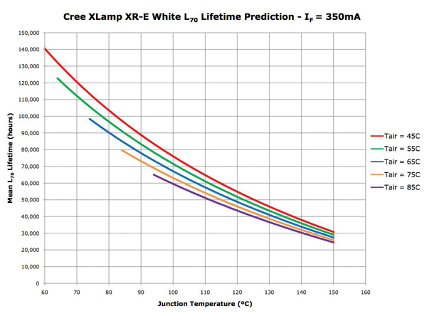
Doubling the junction temperature of an LED from 75°C to 150°C can shorten its life by more than 70 percent (Figure 1: the family of curves represents different ambient temperatures, Tair). Worse still, elevated temperatures reduce the light output from the device for a given forward voltage and forward current.

Figure 1: High-power LED lifetime decreases with increased junction temperature. (Courtesy: Cree.)
LED lighting engineers must consider thermal management strategies. Adding a heat sink will help, but designers should first consider relatively inexpensive modifications to the PCB to improve heat dissipation.
LED junction temperature can be calculated using the following formula:
Tj = Tair + (Rth j-a x Pd)
where:
Tj = Junction temperature (°C);
Tair = Ambient temperature (°C);
Rth j-air = Thermal resistance between the LED junction and ambient (°C/W);
Pd = Power dissipated by LED = Forward voltage (Vf) x Forward current (If) (V x A).
The formula shows that for a device operating at a given ambient temperature, lowering the thermal resistance will bring down the temperature. Simply put, by providing a path for heat to escape, the chip can be kept cooler.
The thermal resistance of an LED lighting assembly is the sum of the thermal resistances of the different materials in the heat path from the junction to the outside world. Let’s assume that a separate heat sink is not part of the design; instead the PCB will double up as the sole heat loss device.
Therefore, the total thermal resistance of the assembly is:
Rth j-air = Rth j-sp + Rth sp-pcb
where:
Rth j-sp = Thermal resistance between LED junction and LED mounting solder pad on the PCB;
Rth sp-pcb = Thermal resistance between solder pad and underside of PCB.
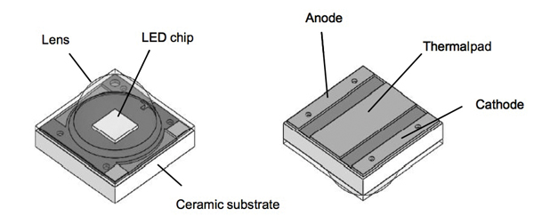
Rth j-sp is determined by the chip packaging supplied by the manufacturer. Figure 2 shows a package for a Cree XLamp XP LED and Table 1 details its thermal resistance in °C/W. While a design engineer has no direct control over Rth j-sp, its value does vary from manufacturer to manufacturer and is an important number to consider when selecting a high power LED. For example, OSRAM offers its OSTAR family which includes high-power white LEDs with Rth j-sp of around 5°C/W.

Figure 2: Cree XLamp XP LED package.

Table 1: Typical thermal resistance (°C/W) values for Cree XLamp LEDs.
Lowering PCB thermal resistance
FR-4, by far the most common substrate for PCBs, is a flame-retardant fiberglass-reinforced epoxy laminate. That makes it a strong, rigid, easy-to-machine material for making circuit boards, but a poor conductor of heat. To demonstrate how bad FR-4’s thermal properties are, let’s calculate its thermal resistance using the formula:
Rth sp-pcb = l/ (k x A) [1]
where:
l = FR-4 thickness (m);
k = Thermal conductivity (W/mK);
A = The area normal to the heat source.
Taking an example where the LED’s thermal pad is mounted on a solder pad on the PCB measuring 10 x 10 mm on a PCB 1.6 mm thick with a thermal conductivity of 0.2 W/mK, the thermal resistance comes out as 80°C/W. (Note that this calculation is an approximation as it doesn’t take into account the conductivity of the interface between LED and PCB, heat spreading, convection thermal resistances, or boundary conditions.)
This is a very high thermal resistance and would likely result in rapid overheating of a high power LED.
But there is a relatively simple modification that can dramatically improve the situation. Adding so-called thermal via holes to the PCB below the solder pad mounting for the LED (Figure 3) lowers the thermal resistance of the substrate. This technique is much more cost effective because many vias are routinely drilled as circuit elements during PCB manufacturing – so adding a few more to the design incurs minimal additional cost.

Figure 3: FR-4 cross-section with thermal vias (not to scale). (Courtesy: Cree)
For best results, LED manufacturers recommend an array of thermal vias situated directly below, and normal to the LED’s thermal pad. This minimizes the resistance by providing several thermal paths working in cooperation as well as limiting heat spreading to the rest of the PCB.
In addition to optimizing the geometry, the efficacy of thermal vias depends on their construction. For example, if the vias are left hollow, they have a higher thermal resistance to those filled with solid copper, solder, or conductive epoxy. Consider a typical 0.6-mm diameter via filled with solder (which typically happens when a copper-plated through via is passed through a soldering machine).
The area of a 0.6-mm-diameter via normal to the LED’s thermal pad is 0.28 mm². The thermal conductivity of solder is about 58 W/mK. Using the formula [1], the thermal resistance of such a via in a 1.6-mm-thick PCB is 97.5°C/W.
Each individual via may not seem to impact heat dissipation but collectively, with several vias under the LED’s thermal pad, the vias will affect the temperature. For instance, if the array comprises five thermal vias, the area normal to the heat source increases by a factor of five and hence the combined thermal resistance drops to 19.5 W/K.
The calculation will be complete when the additional thermal resistance of the FR-4 is considered, because much of the solder pad area is still composed of FR-4.
To keep the calculation relatively simple, assume the thermal resistances of the vias and the FR-4 again act in parallel. The thermal resistance can then be calculated from this formula:
Rth = 1/(1/Rth via + 1/ Rth FR-4)
The result is 15.7°C/W, or 80 percent better than FR-4 alone. (Note: This calculation ignores the area of the solder pad taken up by the vias when calculating FR-4 thermal resistance).
This is a simplified case, which assumes that the underside of the PCB is maintained at a reasonable ambient temperature. In practice, an additional heat sink may be required to dissipate heat from the underside. By adding thermal vias to the PCB and lowering the thermal resistance of the substrate, a smaller, less expensive heat sink could be specified than would otherwise be required.
Reference:
- “Optimizing PCB Thermal Performance for Cree XLamp LEDs,” Technical Note: CLD-AP37.001, Cree Inc.
聲明:各作者及/或論壇參與者於本網站所發表之意見、理念和觀點,概不反映 DigiKey 的意見、理念和觀點,亦非 DigiKey 的正式原則。


