Build Better Video Bridging Solutions
資料提供者:DigiKey 北美編輯群
2017-01-24
Embedded systems developers are taking advantage of innovations in mobile processors, the widespread adoption of the MIPI standard interface, and a new generation of lower-cost image sensors and displays to build in higher performance at a lower cost. Still, there are challenges to be addressed in doing so.
With the rapid rise in performance capabilities how do you predict what type and number of interfaces you will need? How do you take advantage of the innovations these processors offer, yet preserve your often significant investment in legacy displays and/or image sensors? And how can you quickly and cost effectively bridge between different interface types to ensure the success of your design?
This article will describe the implications and design issues associated with migrating to new interfaces and bridging from new to legacy devices, before introducing some possible solutions and how to go about applying them.
Bridging legacy and new video interfaces
The demand is growing for innovative, low-cost video bridging solutions. Designers building surveillance systems, drones or DSLR cameras for instance, want to take advantage of the latest innovations in popular mobile application processors (APs). To do so they must often convert the signal from proprietary, legacy, image sensor interfaces to the mobile MIPI CSI-2 image sensor interface found on most APs.
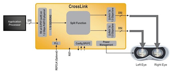
In the case of designers building next generation virtual reality (VR) headsets, they need to convert video coming from a single MIPI DSI interface and split it across two MIPI DSI displays. With one for each eye, this improves system performance and makes products more immersive (Figure 1). But how do you support these emerging applications if the AP only features a single DSI interface or one of the available interfaces is already dedicated to another function?

Figure 1: Video bridging solutions can be used to expand the number of ports on a legacy applications processor or to increase bandwidth and overall performance capabilities. (Source: Lattice Semiconductor)
Similarly, developers of human machine interface (HMI) solutions or smart displays may want to preserve their large investment in industrial displays. But to do so, they must bridge from OpenLDI/LVDS or proprietary interfaces to the CSI-2 interface on their mobile AP.
In other cases you may want to aggregate multiple video streams into a single larger frame output to create depth perception or an augmented reality system. In this situation, you’ll need a bridging solution that sits between your camera sensors and image processor that can capture multiple CSI-2 outputs at the exact same point in time with minimal latency. That will require general purpose pin control. Your multiple merged video streams will also need to share a common clock, and in some cases, may require individual power up routines. To implement each of those functions, you’ll need I/O you can easily customize.
The use of MIPI mobile processors has even reached such traditional industrial applications as auto manufacturing. Advanced driver assistance systems (ADAS) and infotainment subsystems in automobiles need more video bridging capabilities as the electronics content and the number of cameras in automobiles continues to grow.
Originally developed to help the driver see when backing up, cameras are now being used by manufacturers to provide vision on all sides of the vehicle. For instance, some automakers are now replacing side mirrors with cameras to reduce wind resistance and improve fuel efficiency. Designers building video bridging solutions allow manufacturers to aggregate data from multiple image sensors and deliver it to the AP via a single CSI-2 interface.
General purpose switches
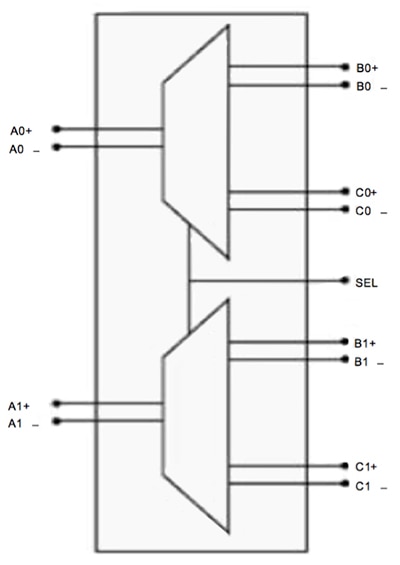
To address the need for basic bridging solutions, designers have typically turned to general purpose type switches. Texas Instruments’ HD3SS3212 is a good example of a general purpose 2-channel mux/demux passive switch used to route signals between two locations on a circuit board (Figure 2). Compatible with MIPI DSI/CSI, FPDLinkII, LVDS and PCIE Gen IIII standards, the device supports data rates up to 10 Gbps.

Figure 2: Functional block diagram for Texas instruments’ HD3SS3212 2-channel mux/demux passive switch that can be used to route signals on a circuit board at rates of up to 10 Gbps. (Source: Texas Instruments)
Designers can use the device in any interface applications requiring a common-mode voltage range of 0 to 2 V with differential amplitude up to 1800 mVPP. Adaptive tracking keeps the channel unchanged for the entire common mode voltage range.
The HD3SS3212 comes with a wide range of tools and support software, including evaluation modules and boards for USB Type-C Minidock boards and reference designs with video and charging support.
Programmable solutions
Another path around the problem is to use semi-custom or custom video bridging solutions. However, these are typically focused on relatively narrow applications and have a long development cycle and the high non-recurring engineering (NRE) costs typical of ASICs.
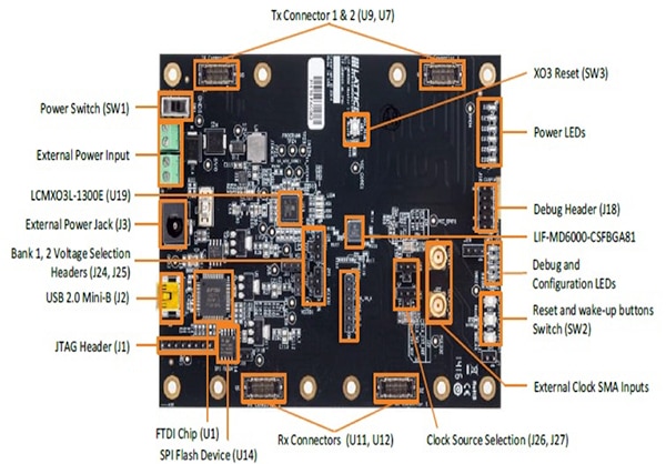
To bridge the gap between general purpose and custom video bridging solutions, you need a video bridging device that combines the design flexibility and short development cycle of an FPGA, as well as the functional performance of an application-specific standard product (ASSP). For these attributes, let’s take a look at the Lattice Semiconductor CrossLink LIF-MD6000 Master Link evaluation board and its programmable ASSP (pASSP) (Figure 3). The CrossLink LIF-MD6000 comes with the eval board as free IP in Lattice’s Diamond design software. Each pASSP surrounds two MIPI D-PHY hard blocks with a mobile FPGA fabric. Each MIPI D-PHY block on the device features up to four data lanes and a clock to support transmit and receive (Tx and Rx). The D-PHYs deliver up to 4K ultra-HD resolution at up to 12 Gbits/s. Two banks of programmable I/O support a good array of interfaces and protocols, including MIPI D-PHY, MIPI CSI-2 and MIPI DSI, as well as CMOS, RGB, MIPI DPI, MIPI DBI, subLVDS, SLVS, LVDS, and OpenLDI.
The adjacent FPGA fabric features 5,936 LUTs, 180 Kbits of block RAM, and 47 Kbits of distributed RAM. The LUTs are arranged alongside dedicated registers in programmable functional units (PFUs) that serve as the basic building blocks for logic, arithmetic, RAM and ROM functions. A programmable routing network connects the PFU blocks.

Figure 3: The CrossLink LIF-MD6000 Master Link board allows you to quickly develop custom video interfacing solutions and configure CrossLink IP with Lattice’s Diamond software. (Source: Lattice Semiconductor)
Rows of sysMEM Embedded Block RAM (EBR) with programmable I/O banks, embedded I2C and embedded MIPI D-PHY are interspersed between rows of PFUs. You can use Lattice’s Diamond design software to configure the PFU blocks and route each design.
For the configuration and setup process, you can select from a wide variety of supporting tools and software. Besides the bridging device, the LIF-MD6000 Master Link evaluation board adds a Mini USB Type-B connector to FTDI, an FTDI to CrossLink circuit using SPI, FTDI to X03LF device using JTAG and GPIO resources. It also gives you access to multiple demos, information on optional Tx/Rx link boards and other documentation. The kit also includes two interface boards, the LIFMD-IOL-EVN SMA IO link interface board and a breakout IO Link board. In addition, the LIF-MD6000 Raspberry Pi boards include a reference design and CrossLink soft IP to interface two Raspberry Pi image sensors to a Raspberry PI processor board.
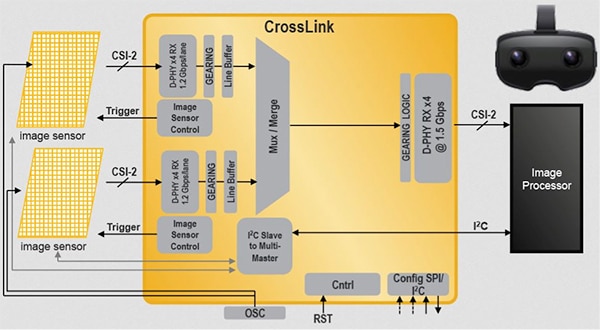
To simplify and accelerate development, Lattice Semiconductor offers pre-engineered soft IP modules for four typical video bridging solutions. The first shows you how to bridge multiple CSI-2 image sensors into a single CSI-2 output (Figure 4). You can use this type of solution in applications where the AP in a design does not offer enough interfaces to support the number of image sensor inputs, or when there is a processing latency between image sensors and imaging data.

Figure 4: Preconfigured soft IP offers designers a simplified solution for converting the input from two MIPI CSI-2 image sensors used to create depth perception to a single MIPI CSI-2 interface on the image processor. (Source: Lattice Semiconductor)
A second solution focuses on 1:2 and 1:1 DSI display interface bridges. This IP targets those environments where rising bandwidth requirements exceed display capabilities while processors continue to offer high performance interface capabilities. By replacing older displays with newer ones, you can upgrade your design while retaining your significant AP investment. This bridge can also be used to extend the output from a single source to two DSI displays instead of one.
The third sample solution provides the key IP for a CMOS to MIPI D-PHY interface bridge using the LIF-MD6000 device. While the MIPI D-PHY was originally developed to address camera and display interconnects in smartphones, many processors and displays today still feature RGB, CMOS or MIPI D-PHY interfaces. This solution serves as a bridge between processors with an RGB interface and displays with a MIPI DSI interface or cameras with a CMOS interface and processors with a CSI-2 interface.
The fourth camera interface bridge solves a mismatch between APs and older image sensors. While many APs now feature the MIPI CSI-2 interface, some high-resolution image sensors use a proprietary sub LVDS output format. This bridge eliminates the incompatibility between those two interface types. This bridge can also be used to convert to or from LVDS, CSI-2, HiSPi and other formats.
Conclusion
As designers increasingly use components originally developed for mobile handsets in a wider array of applications, they often find that devices in their system do not interface to each other directly. Sometimes the type or number of interfaces on the AP does not match those on the system’s image sensors or displays.
For some basic mux/demux applications, standard off-the-shelf analog switches may suffice. But as designers take on tougher bridging tasks, such as converting incompatible interfaces, combining multiple video streams, or splitting video streams into multiple interfaces, programmable FPGA-based bridging solutions offer a number of advantages.
First and foremost, they allow you to leverage existing investments in legacy devices, even while you migrate your design to new APs, image sensors and displays with MIPI interfaces. Secondly, by allowing you to bridge across a wider range of devices with different interfaces, these bridging solutions give you the option of using a broader choice of components. Ultimately, you gain greater design flexibility.

聲明:各作者及/或論壇參與者於本網站所發表之意見、理念和觀點,概不反映 DigiKey 的意見、理念和觀點,亦非 DigiKey 的正式原則。


