


TVS Diodes
Protect your designs with our broad range of transient voltage suppressors
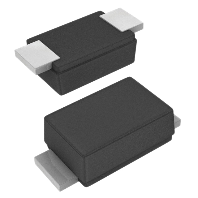
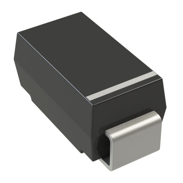
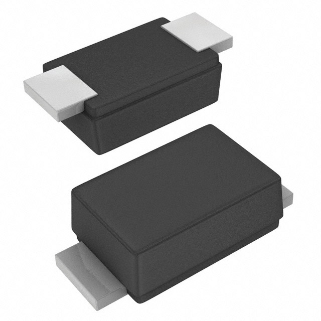
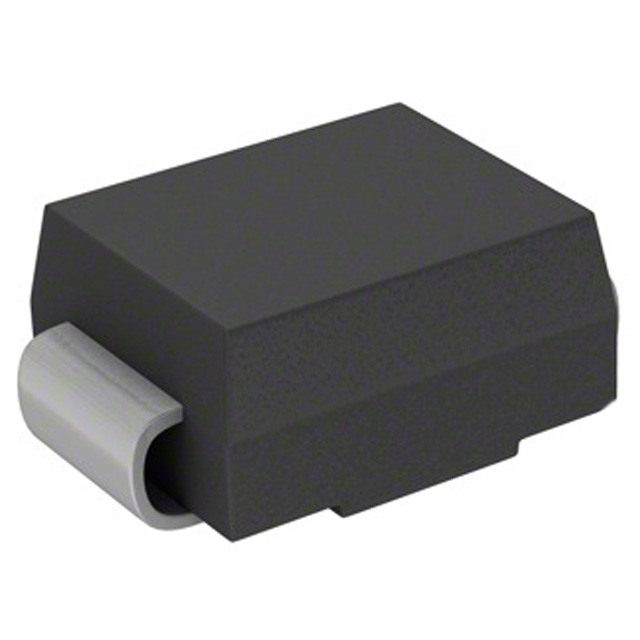
Littelfuse TVS Diodes are designed to protect electronic circuits from damaging overvoltage transients. TVS Diodes are silicon avalanche devices typically chosen for their fast response time, low clamping voltage, lower capacitance and low leakage current. They are ideal for applications in computing, industrial, automotive, telecom and avionic markets. Littelfuse offers these overvoltage protection devices in a wide range of surface mount and axial leaded packages, and peak pulse ratings from 200W (10/1000) to 30kW (10/1000) and beyond (20kA 8/20).
- TVS Diodes
- Buy Now
What are TVS diodes and how do they compare?
TVS diodes are electronic components designed to protect sensitive electronics from high-voltage transients. They can respond to overvoltage events faster than most other types of circuit protection devices and are offered in a variety of surface mount and through-hole circuit board mounting formats.
The device functions by limiting voltage to a certain level (referred to as a “clamping” device) with p-n junctions that have a larger cross-sectional area than those of a normal diode, allowing the TVS diode to conduct large currents to ground without sustaining damage.
TVS diodes are generally used to protect against electrical overstress such as those induced by lighting strikes, inductive load switching, and electro-static discharge (ESD) associated with transmission or data lines and electronic circuits.
While Littelfuse TVS diodes can fit a wide range of circuit protection applications, they were primarily designed to protect I/O interfaces in telecommunication and industrial equipment, computers, and consumer electronics.
Characteristics of the Littlefuse TVS diode include:
- Low incremental surge resistance
- Unidirectional and bidirectional polarities available
- Reverse standoff voltages range from 5 to 512 V
- RoHS compliant–matte tin Pb-free plated
- Surface-mount power ratings from 200 W to 5,000 W
- Axial lead power ratings from 400 W to 30,000 W (30 kW)
- High Power current protection available for 3 kA thru 10 kA
- AEC-Qualified on select series
Comparison to other diode technologies
| Diode Class | Application | Remarks |
|---|---|---|
| Conventional Diode, Rectifier | Power Control | Useful for “steering” high currents; converting AC to DC. Typically found in large packages such as TO-220. |
| Zener Diode | Power Control | Useful for the regulation of DC voltage in power supplies. Typically found in medium to large size packages (axial, TO-220). |
| Silicon Avalanche Diode (SAD), Transient Voltage Suppressor (TVS) | Overvoltage Protection | Useful for protecting circuits exposed to high-energy events such as lightning surges or voltage transients from the mechanical switching of electrical circuits (EFT). Typically found in medium-size packages (axial, DO-214). |
| Diode Array | Overvoltage Protection | Diode arrays fall into the broader category of Silicon Protection Arrays (SPA), which are targeted for ESD protection. Typically found in small surface-mount packages (SOIC-8, SOT-23, SC-70, etc.). |
| Schottky Diode | Power Control | Useful for high-frequency (HF) rectification required for switch-mode power supplies. |
| Varactor Diode | RF Tuning | Only known application of diodes that takes advantage of the junction capacitance characteristic. |
Comparison by operating characteristic
| Diode Class | Reverse Breakdown Voltage (VBR, VZ) |
Capacitance (CJ) | Remarks |
|---|---|---|---|
| Conventional Diode, Rectifier | 800-1500V | Very High | AC to DC power conversion |
| Zener Diode | Up to 100V | Medium to High | DC power regulation |
| Silicon Avalanche Diode (SAD) | Up to 600V | Medium | Lightning surge and voltage transient protection |
| Diode Array | Up to 50V | Low (< 50pF) | ESD protection of high-frequency data circuits |
Comparison by device construction
A Schottky diode is formed by a metal to semiconductor junction. Electrically, it conducts by the majority carrier and possesses fast response with lower current-leakage and forward bias voltage (VF). Schottky diodes are widely used in high frequency circuits.
Zener diodes are formed by a heavily doped P-N semiconductor junction. There are two physical effects that can be referred to as a Zener state (Zener effect and Avalanche effect). Zener effect occurs when there is a low reverse voltage applied to the p-n junction that conducts due to quantum effect. Avalanche effect occurs when a larger than 5.5 volt voltage is applied reversely to the p-n junction during which the generated electron-hole pair collide with the lattice. Zener diodes based on the Zener effect are widely used as voltage reference sources in electronics circuitry.
A TVS diode is formed by a specially designed P-N semiconductor junction for surge protection. The p-n junction is usually coated to prevent premature voltage arcing during a non-conducting state. When there is a transient voltage event, the TVS diode conducts to clamp the transient voltage using the Avalanche effect. TVS diodes are widely used as an overvoltage circuit protection device in telecommunications, general electronics, and digital consumer markets for lightning, ESD, and other voltage transient protection.
SPA stands for Silicon Protection Arrays. It is a diode array of integrated p-n junctions, SCRs, or other silicon protection structures packaged in multi-pin structures. The SPA can be used as an integrated solution for ESD, lightning, and EFT protection for telecommunications, general electronics, and digital consumer markets where multiple protection opportunities exist. For example, it can be used for HDMI, USB, and Ethernet port ESD protection.
Find a part
Surface Mount - Standard & Automotive (AEC-Q) Applications (200-600 W)
SMF
- Package Type: SOD-123
- Voltage: 3.3-250
- Power Range: 200 W
SMAJ
- Package Type: DO-214AC
- Voltage: 5-440
- Power Range: 400 W
SMF4L
- Package Type: SOD-123FL
- Voltage: 5-250
- Power Range: 400 W
TPSMF4L
- Package Type: SOD-123FL
- Voltage: 5-85
- Power Range: 400 W
P4SMA
- Package Type: DO-214AC
- Voltage: 5.8-495
- Power Range: 400 W
SACB
- Package Type: DO-214AA
- Voltage: 5-50
- Power Range: 500 W
TPSMA6L
- Package Type: DO-221AC
- Voltage: 5-85
- Power Range: 600 W

SMA6L
- Package Type: DO-221AC
- Voltage: 5-250
- Power Range: 600 W
TPSMB
- Package Type: DO-214AA
- Voltage: 7.02-553
- Power Range: 600 W
SMBJ
- Package Type: DO-214AA
- Voltage: 5-440
- Power Range: 600 W
P6SMB
- Package Type: DO-214AA
- Voltage: 5.8-512
- Power Range: 600 W
Surface Mount - Standard & Automotive (AEC-Q) Applications (1000-5000 W)
1KSMB
- Package Type: DO-214AA
- Voltage: 5.8-153
- Power Range: 500 W
SMCJ
- Package Type: DO-214AB
- Voltage: 5-440
- Power Range: 1,500 W
TPSMC
- Package Type: DO-214AB
- Voltage: 10.2-256
- Power Range: 1,500 W
1.5SMC
- Package Type: DO-214AB
- Voltage: 5.8-553
- Power Range: 1,500 W

TPSMD
- Package Type: DO-214AB
- Voltage: 10-400
- Power Range: 3,000 W

SMDJ
- Package Type: DO-214AB
- Voltage: 5-440
- Power Range: 3,000 W
5.0SMDJ
- Package Type: DO-214AB
- Voltage: 12-440
- Power Range: 5,000 W
Axial Leaded - Standard & Automotive (AEC-Q) Applications (400-5000 W)
P4KE
- Package Type: DO-41
- Voltage: 5.8-495
- Power Range: 500 W

SA
- Package Type: DO-15
- Voltage: 5-180
- Power Range: 500 W
SAC
- Package Type: DO-15
- Voltage: 5-150
- Power Range: 500 W

P6KE
- Package Type: DO-15
- Voltage: 5.8-512
- Power Range: 600 W
TP6KE
- Package Type: DO-204AC
- Voltage: 11.1-77.8
- Power Range: 600 W
1.5KE
- Package Type: DO-201
- Voltage: 5.8-512
- Power Range: 1,500 W
TP1.5KE
- Package Type: DO-201
- Voltage: 10.2-40.2
- Power Range: 1,500 W
LCE
- Package Type: DO-201
- Voltage: 6.5-90
- Power Range: 1,500 W
5KP
- Package Type: P600
- Voltage: 5-350
- Power Range: 5,000 W

TP5KP
- Package Type: P600
- Voltage: 11-60
- Power Range: 5,000 W
High Power & Automotive (AEC-Q)
SLD
- Package Type: P600
- Voltage: 10-60
- Power Range: 5,000 W

SLD8S
- Package Type: SMTO-263
- Voltage: 12-64
- Power Range: 7,000 W
15KPA
- Package Type: P600
- Voltage: 12-280
- Power Range: 15,000 W
20KPA
- Package Type: P600
- Voltage: 20-300
- Power Range: 20,000 W
30KPA
- Package Type: P600
- Voltage: 28-360
- Power Range: 30,000 W

LTKAK6
- Package Type: SMTO-218
- Voltage: 58-76
- Power Range: 6,000 kA

LTKAK10
- Package Type: SMTO-218
- Voltage: 58-86
- Power Range: 10,000 kA

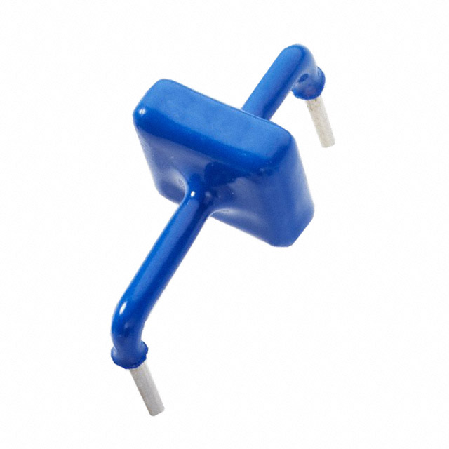
AK3
- Package Type: Radial Lead
- Voltage: 15-430
- Current: 3,000 kA
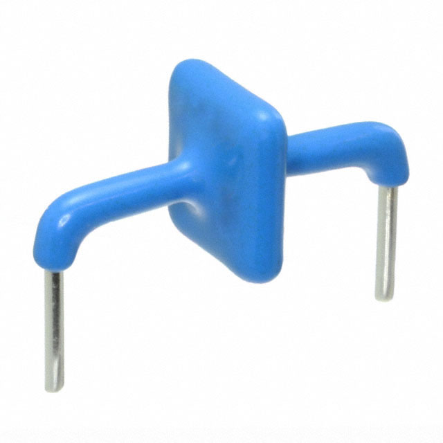
AK6
- Package Type: Radial Lead
- Voltage: 30-430
- Current: 6,000 kA
AK10
- Package Type: Radial Lead
- Voltage: 58-530
- Current: 10,000 kA

AK15
- Package Type: Radial Lead
- Voltage: 58-190
- Current: 15,000 kA

