

What Is Power Converter Deadtime and How Can I Control It?
Increasing power requirements in automotive, small electric vehicles (EVs), cordless tools, and charging stations are driving the move to 48 volt power systems. These systems offer the benefits of higher efficiency and lower losses, as well as smaller size and weight. All of these power systems convert the power supplied by the 48 volt bus into usable voltages, requiring the use of power converters.
Power converters use switched power techniques to convert 48 volts DC into selected voltages. A typical 48 volt converter, in this case, the Texas Instruments’ UCC28251PWR, is based on half-bridge-configured power switch devices like field-effect transistors (FETs), shown as Q1 and Q2 in Figure 1. These are controlled by a pulse width modulation (PWM) controller to produce and regulate the desired output voltage.
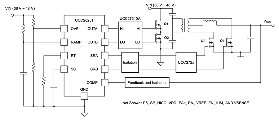 Figure 1: A typical DC-DC converter uses a PWM controller to drive half-bridge-configured power FETs. The controller adjusts the pulse width at the FET inputs to produce and regulate the required voltage at the output (VOUT). (Image source Texas Instruments)
In this circuit, the FETs, Q1 and Q2, form a half-bridge topology. They are turned on alternately to drive the transformer. The FETs Q3 and Q4 are synchronous rectifiers that convert the switching waveform from the transformer secondary back to DC. Synchronous rectifiers eliminate the series voltage drops associated with semiconductor rectifiers, thereby improving efficiency. These rectifier FETs must be driven synchronously with the primary power switching devices.
Alternative inverter topologies include the full, or “H” bridge, using four FETs, or the six-FET cascaded full-bridge, which is used for three-phase converters. All of these technologies use one or more pairs of power devices. The pairs are serially connected, like the FETs in Figure 1.
There are two critical issues with any of these topologies. The first is that the switching device on the high side (Q1) and the low side (Q2) can never be allowed to be on at the same time. If that occurs, there is a short circuit between the 48 volt bus and ground. This condition is called shoot through, and it usually damages the power switches. Shoot through is prevented by controlling the switching times for each power device independently. The goal is to have the active device turn off before the inactive device is turned on.
The delay between the two events (turn on and turn off) is called primary deadtime. It is measured by comparing the transition times of the gate-to-source voltage (VGS) of the high side and low side FETs at the maximum controller pulse width (Figure 2). The delay between both sets of transitions is deadtime.
 Figure 2: Primary deadtime is measured by comparing the transition times of VGS of the high side and low side FETs at the maximum controller pulse width. The delay between both sets of transitions is deadtime. In this example, it is 1.498ns and 1.166 ns. (Image source: Art Pini)
In Figure 2, the delay between the low side FET (VGS LO) turning off and the high side FET (VGS Hi) turning on, is 1.498 ns. The other condition is that where the high side FET turns off and the low side FET turns on, a delay of 1.166 ns. If both of these measured delays are positive, the deadtime is acceptable. Note that this measurement is made at the maximum pulse width of the PWM controller output.
During the deadtime, neither device is conducting; this constitutes a ‘deadtime’ loss. Like all losses, it’s increasingly important to keep them to a minimum.
A second critical issue is to coordinate the operation of the synchronous rectifiers with the primary switching operations.
The UCC28251PWR controller shown in Figure 1 can control either half or full-bridge circuits and provides both gate drive signals and the synchronous rectifier outputs with programmable delays. The UCC28251PWR controls the primary-side deadtime and also includes cycle-to-cycle overcurrent protection. The delays between the primary outputs and the secondary synchronous rectifier drive signals, referred to as secondary deadtime, are independently programmable via two external resistors.
The PWM controller is used in conjunction with a primary-side half-bridge gate drive IC, the Texas Instruments UCC27210DDAR. This IC drives both of the gate-source inputs of the two N-channel FETs in this half-bridge configuration. It affects the primary deadtime due to its inherent propagation delay, which is 18 ns (typical). The propagation delay issue is minimized by matching the delay between both gate drive outputs. The UCC27210DDAR gate driver IC has its outputs matched to within 2 ns. A gate driver of the same family with similar timing characteristics is used to drive the synchronous rectifier FETs.
Conclusion
Moving to 48 volt systems has inherent advantages with respect to efficiency, size, and weight, but designers need to understand the cause of deadtime and how to minimize it. As shown, special-purpose ICs are available with the functions necessary to safeguard the operation of 48 volt power converters. They control both primary and secondary deadtimes, eliminating the main possible problems for both half and full-bridge circuit topologies.
About this author

Arthur (Art) Pini is a contributing author at DigiKey. He has a Bachelor of Electrical Engineering degree from City College of New York and a Master of Electrical Engineering degree from the City University of New York. He has over 50 years experience in electronics and has worked in key engineering and marketing roles at Teledyne LeCroy, Summation, Wavetek, and Nicolet Scientific. He has interests in measurement technology and extensive experience with oscilloscopes, spectrum analyzers, arbitrary waveform generators, digitizers, and power meters.

Have questions or comments? Continue the conversation on TechForum, DigiKey's online community and technical resource.
Visit TechForum and the INTERNET350U Desktop UPS (right)")


