Battery Booster ICs Elegantly Extend the Life of Lithium Coin Cells in Wireless Applications
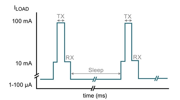
The Internet of Things (IoT) has accelerated the proliferation of wireless sensors. Whether for consumer, medical, industrial, or agricultural, these sensors must be small, lightweight, and have a long battery life. Also, these devices subject the power sources to intermittent high current loads during transmit and receive modes. For example, transmission bursts can draw 100 milliamperes (mA) while receive operation can draw 10 mA, with much longer periods of lower-current sleep-mode operation in the microampere (µA) range (Figure 1).
 Figure 1: A typical wireless device's load profile shows short intervals of high current demand for transmission (100 mA) and receive operation (10 mA), and much longer periods of lower-current sleep-mode operation. (Image source: Nexperia, modified by author)
The transmit or receive operation period typically has durations in the tens of milliseconds, while the device generally stays in sleep mode for hundreds of seconds. Though the average current is low due to the short duty cycle, the high peak currents pose a problem.
Lithium coin cell batteries are small and have high energy density, but supplying currents upwards of 10 mA can significantly lower their lifetimes. They also have relatively high internal resistance and are inefficient in supplying these higher currents. For example, a new coin cell has an internal resistance of about 10 ohms (Ω). Supplying a current of 100 mA results in a voltage drop of 1 volt across the cell’s internal resistance. Under this heavy load, the cell’s chemical reaction rate also causes the output voltage to drop. Also, as the cell ages, the internal resistance increases. One possible alternative is to use alkaline batteries. These have higher peak current ratings, but their downside is that they are significantly larger than coin cells.
Booster extends coin cell life
Nexperia has developed a clever solution to support the coin cell. Its family of coin cell battery life booster integrated circuits (ICs) isolates coin cells from the high current demands of the RF circuitry. In doing so, they extend the duration of the cells in wireless sensor applications, enabling smaller and lighter packages with excellent battery life.
The boosters use dual DC-DC converter stages. The first stage draws energy at low current from the coin cell to charge a capacitive storage element to a higher voltage than the battery. Once the storage capacitor is charged, the second DC-DC converter supplies on-demand energy to the intermittent load at a regulated output voltage. The coin cell battery is never subject to the high current demanded by the external load, thus extending the battery’s lifetime.
Using this approach, battery lifetimes can be increased from four to ten times in applications with high intermittent load current while increasing the peak output current by as much as 25 times. There are two device families matched to the characteristics of either lithium manganese dioxide (LiMnO2) or lithium thionyl chloride (Li-SOCl2) batteries (Table 1).
|
Device
|
Maximum storage voltage (volts)
|
Maximum load current (mA)
|
Input voltage range (volts)
|
Output voltage range (volts)
|
Interface
|
Battery type
|
Auto start mode
|
|
11
|
200
|
2.4-3.0
|
1.8-3.6
|
I2C
|
LiMnO2
|
Yes
|
|
|
11
|
200
|
2.4-3.0
|
1.8-3.6
|
SPI
|
LiMnO2
|
No
|
|
|
5.5
|
150
|
2.4-3.6
|
1.8-3.6
|
I2C
|
Li-SOCl2
|
Yes
|
|
|
5.5
|
150
|
2.4-3.6
|
1.8-3.6
|
SPI
|
Li-SOCl2
|
No
|
Table 1: Characteristics of the NBM5100/NBM7100 families of coin cell battery life booster integrated circuits. (Table source: Art Pini)
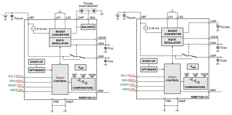
The battery boosters are internally similar (Figure 2).
 Figure 2 : The block diagrams of the NBM5100A/B and NBM7100A/B devices show they are functionally similar. (Image source: Nexperia)
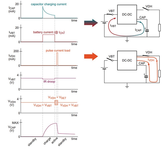
The operation of these coin cell battery boosters is also similar (Figure 3).
 Figure 3 : Shown are graphs of the NBM5100/7100 voltage and current status for the charging (upper right diagram) and active load (lower right diagram) cycles. (Image source: Nexperia)
The cell battery booster uses dual high-efficiency DC-DC converters to buffer the battery from short-duration high-current load transients. In the first conversion stage, a boost converter is used during the charge cycle. This cycle is initiated in advance of a period of heavy load current. When charging, energy is transferred from the battery to an external storage capacitor with a voltage (VCAP) higher than that of the battery cell. The charge cycle draws a low constant current (IVBT) from the battery. Due to its internal resistance, the low charging current produces a drop in the battery output voltage (VVBT). With the capacitor charged, the buck regulator DC-DC converter handles the active cycle, transferring energy from the storage capacitor to the output (VVDH), thus supplying high load current (IVDH) at a regulated voltage with up to 90% efficiency.
Note that the drawn battery current (IVBT) remains very low during the charge cycle and negligible during the active cycle. This decreases the repetitive stress on the battery and extends the cell’s usable capacity. When not in the charging or active cycle, the output drops to a quiescent or standby state, consuming less than 50 nanoamperes (nA).
The cell battery booster ICs use an adaptive learning algorithm that monitors the load pulse characteristics and intelligently optimizes energy transfer and storage to the capacitor. Up to 63 load profiles can be retained to adjust the charging process.
Booster operating modes
The NBM5100/7100 devices operate in continuous, on-demand, and auto mode (NBM5100A and NBM7100A versions only). The continuous mode is used in applications that require an instant response to the transient load. The storage capacitor is charged, and the DC-DC converter is idled. The voltage on the storage capacitor is monitored and refreshed as needed. On receiving an active command, the stored capacitor's regulated output is immediately available. The storage capacitor is recharged after delivering the required energy to the load. When fully charged, the ready signal is set.
The on-demand mode is used for applications requiring maximum battery life. It starts in the standby state. The on-demand mode is initiated using the I/O interface to set the appropriate bit. The storage capacitor is charged when needed, making the stored energy available as indicated by the ready signal.
The auto mode uses the start signal to initiate the on-demand operation without using the I/O interface. The ready signal indicates the storage capacitor is fully charged and available.
The NBM5100/NBM7100 series are controlled using serial I/O interfaces. The NBM5100ABQX and the NBM7100ABQX devices use an I2C interface, while the NBM5100BBQX and the NBM7100BBQX ICs are equipped with SPI interfaces.
These battery life extenders monitor the number of charging cycles and report the remaining charge in the coin cell. They report the battery charge status via a fuel gauge register available through the serial interface.
The NBM5100/NBM7100 series coin cell battery life extenders are available in a SOT763-1 (DHVQFN16) 16-pin package and have an operating temperature range from -40 to +85°C.
Nexperia offers the NEVB-NBM5100A-01 and NEVB-NBM7100A-01 evaluation boards for the NBM5100ABQX and the NBM7100ABQX, respectively. The boards enable quick and convenient evaluation of the battery boosters. They can be connected to a board under development and controlled from a PC over a USB connection using a graphical user interface (GUI).
Conclusion
The NBM5100/NBM7100 battery boosters extend the life of lithium coin cell batteries in wireless IoT applications with high transient loads that might otherwise need to use much larger AA or AAA batteries. As such, they are an elegant way to reduce device size while reducing costs.

Have questions or comments? Continue the conversation on TechForum, DigiKey's online community and technical resource.
Visit TechForum


